Table of Contents
Toggle2.4 GHz PCB antenna layout is a critical aspect of designing wireless devices that operate on this frequency. The layout of the antenna on the PCB can have a significant impact on the device’s range, performance, and overall functionality. Therefore, it is essential to have a good understanding of the best practices for designing a 2.4 GHz PCB antenna layout.
The 2.4 GHz frequency band is commonly used for wireless communication, including Wi-Fi, Bluetooth, and Zigbee. These technologies are used in various applications such as smartphones, laptops, smart homes, and IoT devices. The PCB antenna design plays a crucial role in the performance of these devices, and a poorly designed antenna can result in a weak signal, reduced range, and interference issues. Therefore, it is essential to have a clear understanding of the antenna design principles to ensure optimal performance and reliability of the wireless device.

PCB Antenna Basics
2.4 GHz Frequency Band
The 2.4 GHz frequency band is commonly used in wireless communication systems, including WiFi, Bluetooth, ZigBee, and other IoT devices. This frequency band is also known as the Industrial, Scientific, and Medical (ISM) band. The 2.4 GHz frequency band has a wavelength of approximately 12.5 cm, which makes it suitable for small PCB antennas.
Antenna Types
There are different types of antennas that can be used in PCB designs, including monopole, dipole, patch, and helical antennas. Each antenna type has its own advantages and disadvantages. For example, a monopole antenna is easy to design and has a low profile, but it has a limited bandwidth. A patch antenna has a higher gain and a wider bandwidth, but it requires a larger PCB area.
PCB Antenna Design Considerations
Designing a PCB antenna requires careful consideration of various factors, such as the antenna type, the PCB material, the ground plane, the feed line, and the matching network. The following are some design considerations for PCB antennas:
- Antenna Size: The size of the antenna should be optimized for the desired frequency band and the available PCB area.
- Ground Plane: The ground plane is an important part of the antenna design, as it affects the antenna’s performance and radiation pattern. The ground plane should be large enough and should have a low impedance.
- Feed Line: The feed line should have a low loss and should be impedance-matched to the antenna.
- Matching Network: A matching network may be required to match the antenna impedance to the transmission line impedance.
In summary, designing a PCB antenna requires careful consideration of various factors, including the antenna type, the PCB material, the ground plane, the feed line, and the matching network. By optimizing these parameters, it is possible to design a high-performance PCB antenna for wireless communication systems.
PCB Antenna Layout

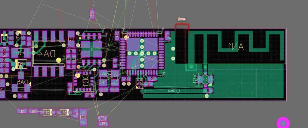
When designing a 2.4 GHz PCB antenna, the antenna layout is a critical factor that can affect the performance of the antenna. In this section, we will discuss the essential elements of PCB antenna layout.
Ground Plane
The ground plane plays a vital role in the performance of the antenna. It acts as a reference plane for the antenna and helps to reduce the radiation pattern towards the ground. The ground plane should be as large as possible to provide a low-impedance path for the antenna current. It is recommended to keep the ground plane uninterrupted beneath the antenna to avoid any reflections.
Antenna Placement
The placement of the antenna on the PCB is another crucial factor in the antenna’s performance. The antenna should be placed as far away as possible from any metallic or conductive objects to avoid any interference. The antenna should also be placed in such a way that it has a clear line of sight to the surrounding environment.
Trace Width and Length
The trace width and length are essential factors in determining the impedance of the antenna. The trace width should be chosen such that it provides the desired impedance for the antenna. The trace length should be kept as short as possible to avoid any losses due to the skin effect.
Matching Network
The matching network helps to match the impedance of the antenna to the impedance of the transmission line. The matching network can be either a series or shunt matching network. The choice of the matching network depends on the impedance of the antenna and the transmission line.
In summary, the PCB antenna layout is a critical factor in the performance of the antenna. The ground plane, antenna placement, trace width and length, and matching network should be carefully designed to achieve optimal performance.
Testing and Optimization

Testing Methods
To ensure the effectiveness of the 2.4 GHz PCB antenna layout, testing is necessary. There are several methods to test the antenna, including:
- S-Parameter Testing: This measures the reflection coefficient, which reflects the amount of power that is reflected back to the source.
- Radiation Pattern Testing: This measures the direction and strength of the radiated signal.
- Impedance Matching Testing: This measures the impedance of the antenna and the matching circuit.
Using a combination of these testing methods can provide a comprehensive understanding of the antenna’s performance.
Optimization Techniques
Once testing is complete, optimization techniques can be used to improve the antenna’s performance. Some techniques include:
- Adjusting the antenna’s physical dimensions: Changing the length, width, or shape of the antenna can improve its performance.
- Adjusting the matching circuit: The matching circuit can be adjusted to ensure that the antenna is properly matched to the transmission line.
- Using a ground plane: Adding a ground plane can improve the antenna’s radiation efficiency.
It’s important to note that optimization techniques should be used carefully and with precision. Making drastic changes to the antenna without proper testing can lead to decreased performance.
In conclusion, testing and optimization are crucial steps in ensuring the effectiveness of a 2.4 GHz PCB antenna layout. By using various testing methods and optimization techniques, the antenna’s performance can be improved.

