What is HDI PCB ?
In the PCB design world, HDI term means High-Density Interconnector. And this kind of PCBs is amongst the designs with fastest-growing which are surfacing. HDI PCB is a term for circuit boards which have a denser wiring per certain area, as a contrary with conventional board. The characteristics of HDI PCB is that it has capture pads and minor vias, finer lines, and spaces, and denser connection pad. These characteristics can enhance electrical performance, also make a lower size and weight of devices or equipments. Moreover, people choose HDI PCB because in
the case of costly covered boards and high-layer amount HDI PCB is the better option. However, although HDI PCB has less transmission times, lighter weight, a signal loss reduction, and more area to put components/parts, it also has few drawbacks when you want to implement the designs
to your device. Moreover, in the real industrial cases if you want to push for a better, stronger, and faster product then it usually implies a force driven by consumer. And there is no difference here. If you want to make your products/devices become more efficient, smaller, lighter, faster, then it resists from this request. In the HDI PCB design case, we are forced to place as many parts into a small area as possible (with high-density) at the same time connect all of them (interconnecting) in an efficient and fast way.
What is HDI PCB
We can imagine an HDI PCB as a “multilayer” cake. For example, we can imagine this is a tasty multilayer rainbow cake. The topping cake layers with some marbles can be imagined become our copper top plane, and the multilayers with various colors become the structural material with nonconductive type, which is usually a kind of fiberglass. On the other hand, the same approach is embodied in the manufacturing of HDI PCBs. Using various layers of fiberglass routing and copper substrates of the alternatively component-littered one-layer boards as the clears up area and
internal in the top layer to put more parts.
Vias in Pad Placement Techniques. HDI boards are depicted with high-density aspects containing micro-vias with laser, fine lines, and high-performance slight materials. It is because the denser PCB design leads to more functions per certain area. At the beginning moments of HDI
PCBs invention, we started with a creative way to ‘obscure’ the routing in each part to relieving area on the top layer. This technique was to put the routing allocation of our electronics design on the underneath of the PCB. The each part pins would hit the fiberglass then be functional on the
backside of the PCB. That’s great! However, related with an even packed board with more density, what’s the explanation? We then know that we are possible to grab this insight and essentially stacking a combined PCB to then use the same technique. This is then, in effect, delivered to us a
various-layers board which had routing plans both in the top layer level, the rear, and also in the center board layer. This moment was the beginning of HDI PCBs which are highly densely packed. The directing insight was when we are able to make a 3-layer board, then why not 4-layer or even six-layer? Then, is the twelve-layer impossible? Then it comes up with VIAS, which are simply something to connect a routing plan which is internal-layered to the other ones. This enables us to hide away layers and routing layers inside of a PCB and even nobody realizes about it.The parts placement on the HDI board requires more precision, comparing to a conventional board design because of fine pitch and miniature pads of the electronics design on the HDI board.
Moreover, leadless ICs need special soldering techniques and additional procedures in between the assembly steps and repair steps. The lesser size and weight of the electronics design of HDI leads to the PCBs match into the small spaces and become lighter than conventional board designs.
The lesser size and weight even implies the existence of a smaller chance of wreck from mechanical disturbances. Since HDI PCBs got more often employed via routing plan they must start applying parallel technology, called pad processes. Technology of pad placement gave an extra point not only for the manufacturing of these chips since they produced it more smooth for routing the pins, yet also the inadequacy of peripheral pins permitted for more placings exactly around the chip implying it a much denser packed circuit. Combining pad ICs with vias permitted for the domestic routing of those circuits to be placed, once more, with nobody ever expecting they were located there. The HDI PCBs obviously can save a secret, even we can believe them with our social media password …
Benefits of using HDI PCB. One of the most frequent background why people utilize HDI PCBs are a valuable improvement in the density of the packaging. The area that achieved by the finer track arrangement exists for components. Moreover, the overall space needed is decreased and will lead to less board sizes as well as fewer layers. HDI technology causes connection and routing easy, particularly if we want to route between pins. HDI PCBs have the advantage of the freshest technologies existing to strengthen the performance of circuit boards through similar or little
amounts of area. This innovation in board technology is encouraged by the tiny semiconductor packages and parts that contribute excellent characteristics in innovative and wonderful new products like touch screen tabs, small transceivers, etc. Some functions which are improved by applying HDI PCB:
a) More stable in power aspect
b) Denser trace routing
c) Increase integrity of signal in designs with high-speed specification
d) Decrease interference inductance and capacitance effects
Speed up our developments with HDI PCBs:
1. Faster routing
2. Easier to put SMD components
3. More component area (also by Pad Via)
4. Decrease frequent relocation of parts/components
Applications. HDI PCB shows one example of the quickest developing technologies in Printed Circuit Boards. Due to its denser circuitry comparing to conventional PCBs, the HDI board design can combine smaller capture pads as well as vias, and more densities of connection pad. HDI Boards comprise blind and planted vias, also often comprise 0.006-micro vias or smaller in diameter size. By utilizing HDI PCB technology, engineers or designers now get the flexibility to put more components or parts on both two sides of itsraw PCB when needed. Currently, since the innovation of pad via and via in blind technology, it permits engineers or designers to put smaller components or parts closer jointly. This leads to less signals transmission time and a valuable decrease in crossing delays and signal loss. Related with the electrical requirements of signals with high-speed specification, the board ought to have different aspects such as impedance control, reductions redundant radiation, high-frequency transmission capability, etc. Moreover, to the outcome of the fine pitch package, assembling methods of leadless, and bonding of direct chip, even the boards are displayed with incredible high-density. Numerous advantages are linked with HDI board, such as small size, high-frequency, and high-speed. HDI board is commonly discovered in devices with touch-screen, mobile phones, 4G network communications, digital cameras, laptop computers, and also prominently found in various medical devices. Now, HDI board is widely utilized in some end-user devices such as game consoles, MP3 players, etc.
Request HDI PCB Quote, Pls send PCB file to Sales@raypcb.com Now
HDI PCB Stackup
If we want to talk about PCB stackups, then firstly we should also say that the manufacturers have three approaches that they refer to during the assembly process. These approaches are:
• Standard/regular lamination, which involves using stratified thru-holes or vias;
• Utilizing plated through, buried, and blind vias for sequential lamination; and
• Utilizing microvias for lamination buildup.
Between these three approaches, the third approach is particularly appropriate for HDI PCB. Some HDI PCB manufacturers suggests utilizing microvias for lamination buildup in HDI PCBs whose BGA pin type is subtantial pin-count and other packages with fine-pitch since benefits and
drawbacks come to each kind of it. Similarly, a sequential lamination using buried and blind vias possibly has not sophisticated via models and lesser via stubs, and also with lesser via diameters comparing to those needed for thru-hole vias. Although sequentially laminated boards are more
expensive than the regular lamination with thru vias, it preserves the similar minimal width of trace and also their applicable reliability restricts their layers up to 2 or 3 layers. Restrictions above are implying to a bigger amount of HDI board manufacturers changing to establishing laminations using microvias and also other sophisticated aspects for HDI boards. Utilizing microvia in HDI board design leads to some benefits such as obtaining very large route density yet with fewer number of layers since the vias and traces have much lesser dimensions relatively. In the microvia HDI boards, the possibility for fewer layers is coming from effectiveness in the utilization of patterns using microvias, since this enables larger space to route, giving the only usable approach of designing using several big and BGAs with fine-pitch in 0.8 millimeters or below. Providing the high-density PCBs yet also the cheapest cost for the highfrequency at the same time, HDI PCB technology, with appropriate stackup term, also enhances signal and power integrity to high-frequency boards. Even though in processes requiring RoHS particular materials fabricators utilized for HDI boards perform well, utilization of recent materials lead to the possibility of higher outcomes with the cheapest costs. Particularly, these recent material types are not fit for the boards fabrication using either sequential or regular lamination.
Different types of HDI stackups. It is suggested in one of a standard (IPC-2315) that manufacturers utilize one from six various stackups types for HDI PCBs. These types are categorized from type I to type VI. Nevertheless, the type categorized with IV and above probably not becomes a good option for HDI board because of some consequent problems. One of them is the manufacturing expense, which causes it as an inappropriate plan for mass manufacture. Furthermore, there are particular design and also assembly obstacles in which the PCB vendors still have not discovered the satisfying solution. Because of the design and price obstacles, in this part, we will only discuss an HDI Stackup types I, II, and III. And here are the details of the three types.
1. HDI Stackup Type I
When you observe at the board structure, you will realize that there is a covered core with 1 or more microvias layers. These multilayers can be put on both two sides, despite possible on a one side. Although the regular Type I does not permit you to put buried vias, you are allowed to employ PTH vias and blind. And for the number of total layers, you should examine that continuing with thin dielectrics (FR-4) probably imply to delamination below tremendous heat, which probably be required to embody lead-free technique of soldering. Moreover, the ratio of length with hole diameter probably be important for reliability, also you ought to always maintain that ratio below 10 in the plated thru-hole.
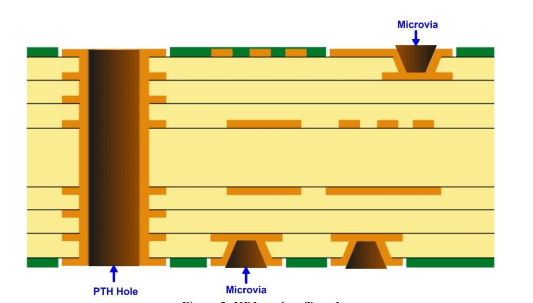
Figure 2: HDI stackup Type I
The characteristic of HDI stackup Type I is an arrangement of a covered core with a one layer (at least) of microvias, either on one of the sides or the two sides. HDI PCB stackup Type I probably utilize blind vias and PTH vias, although it is not buried vias. There are two factors that restrict the layer amount of the covered core in HDI PCBs Type I:
FR-4 dielectrics with very thin characteristics can delaminate under high-temperatures
needed for lead-free soldering.
The ratio factor or total of length to the hole diameter in the plated PTH thru-hole via have to be smaller than 10 for keeping reasonable reliability. Consequently, HDI stackup Type I will not become remarkably more preferable than the cover for high-dense boards which have various BGAs with pin-count, because the via pads of PTH will require to increase its dimension for bigger counts of layer. Additionally, the utilization
of a microvia with single layer will not provide decent advantages with the special aspects introduction such as fewer thinner traces and diameter vias.
2. HDI Stackup Type II
In the HDI stackup type II, you can utilize blind and buried vias, and also microvias on a covered core. And you also require to put 1 or more microvias layers at the sides. Additionally, you are not required to place them in both two sides, however at least 1 is necessary. Manufacturers sometimes undergo with staggering or stacking them. It depends on buried vias, and probably they stagger microvias from other ones. The experts examine that this technique is much more appropriate for boards with high-density spec, however you ought to remember the same constraints as with the HDI type I stackup method. Then you are only be able to put microvias in outside layers, that leads to certain constraints for some projects.
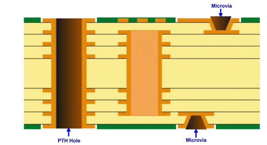
Figure 3: HDI stackup Type II
Moreover, HDI stackup Type II arrangement utilizes microvias, buried and blind vias laid on a covered core, with a one layer (at least) of microvias, either on one of the sides or both of the sides. Manufacturers probably jiggle certain microvias in between other microvias, then heap them or jiggle them near buried vias. Even though the HDI stackup Type II is remarkably better comparing to the HDI Type I in high-dense boards utilizing various fine-pitch parts, but its constraints are similar just like the HDI stackup Type I for the aspect of the constraints in the amount of covered core layers. Since HDI PCB stackup Type II probably has the microvias only in the layers at outermost, it puts constraints on utilizing the layers at outermost as a power or ground plane. Moreover, this is not significantly effective when for trace routing you only have a single layer with buildup.
3. HDI Stackup Type III
The fundamental difference between HDI type II stackup and type III stackup is that in this approach, you need to put 2 or more microvias layers in the sides and you are not required to put them in both two sides. Moreover, you have blind and buried vias, and also microvias, on a covered core. This stackup configuration could be a good option for PCBs with high-density which have many layers and utilize various big BGAs whose features are fine-pitch. In the thin FR-4 dielectrics as well as PTH holes, then the similar constraints will exist. The significant benefit of HDI type III stackup is which you are able to utilize the layers in outside for ground and power planes. You can obtain that by putting microvias in inner layers, that is purposely to make sure that the manufacturers have adequate layers to be utilized for routing of signal. When you are ok with the more expensive cost, you probably also utilize vias with stacks for amazing routing density.
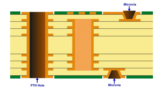
Figure 4: HDI stackup Type III
HDI stackup Type III arrangement also utilize microvias, buried and blind vias in a covered core, using two layers (at least) of microvias, either on one of the sides or both of the sides.Manufacturers probably jiggle certain microvias in between other microvias, then heap them or jiggle them near buried vias. HDI PCBs Type III provide the optimum stackup arrangement for high-dense PCBs with multilayers using various big BGAs that have fine-pitch features, even though their constraints are similar on the amount of layers like occurred in HDI stackup Type I, as well as Type II stackup, when they utilize holes in PTH and thin dielectrics (FR-4). Utilizing the layers at inner microvias of HDI PCBs Type III enables the layers at outer to be utilized for power and/or ground planes, remaining a sufficient amount of layers used for routing the signal. Moreover, engineers or designers can achieve higher stacked vias in routing density, but at a more expensive cost. Lastly, it depends on your available budget and the application you are aiming, your engineers or designers probably utilize some of the 3 types of HDI board stackups. The microvias of HDI Type
III provide the broadest kind of via spans and models. Manufacture cost will vary since it depends on the optimum via models which have the highest signal integrity and route density.
HDI PCB Design
PCB Design Considerations. Before designing HDI PCB we should consider some common aspects into our HDI PCB design:
Thermal: HDI often increases the thermal performance while you still want to consider the thermal stability of microvias and trace widths in high-speed signal designs.
EMI/EMC: All those radiation constraints such as preventing accidental antennas and practical noises, particularly as HDI is utilized for high-speed signal designs.
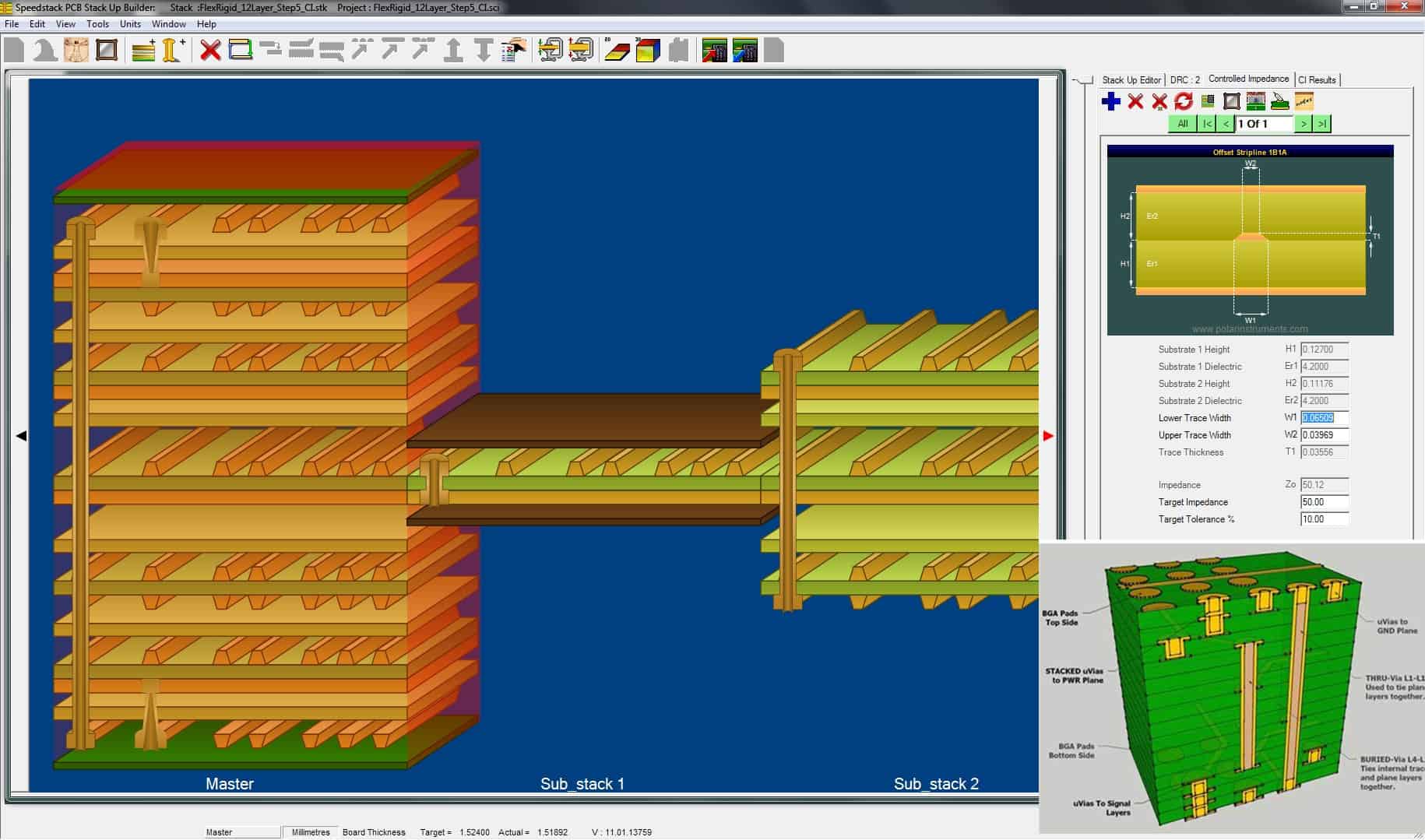
Impedance Control: You will need to manage tight tolerances (within ±10%) on dielectric layer thicknesses, spacings, and trace widths to make sure the impedance does not influence signal integrity.
The need to factor thermal, electromagnetic, and physical constraints into an HDI PCB design appends a lot of complexity to the design process. However, some EDA (electronic design automation) software tools have been developed to reduce the complexity of solving multidimensional PCB problems.
Tips for Designing HDI PCB Boards. Designing PCB layout may be somewhat complex in which the designers need to make hard resolve related with aspects to be considered as the most important ones. Then the process becomes more sophisticated when we design PCB for a crucial
systems like automotive, medical devices, military, or aerospace, and for systems with highperformance things like IoT and HDI boards. Inconsiderate of the board design type, the top manufacturing outcomes are achieved when the engineer or designer combines strategy of DFM
that targets advantages to development of PCB and also is adapted with the abilities of their contract manufacturer (CM). DFM is a collection of regulations and guidelines which target a particular stage of manufacturing process like a DFA and DFT. DFM also can be concerned with a particular type of board design like HDI PCB boards. Now, let’s discusssome fundamental design tips which are aimed for optimizing HDI PCB boards manufacturing.
Glossary
DFM: Design for manufacturing
DFA: Design for assembly
DFT: Design for testability
1. Select types of via to minimize complexity of the process
The vias option is a crucial resolve which not only defines the manufacturing and equipment procedures needed but also influences time of the processing and extra costs. The utilization of buried or blind, microvias, helps to decrease the material costs and amount of layers; nevertheless, the option of if to utilize pad via, near vias in pad or dogbone influences the process complexity.
2. Select a minimal amount of components/parts to employ HDI
The components selection is always crucial; nevertheless, the optimization of component selection is more important for HDI PCB boards. The parts for your design of the HDI PCB define trace locations, widths, sizes, and types for stackup and drill holes. Explicitly, performance ability is a prominent concern. However, traceability, availability, and packaging should be noticed also. Having to replace parts or redesign current layout can boost up the extra manufacturing material costs and time.
3. Give distance components/parts to minimize tension and EMI
At the point when a component position is with the end goal that via positions are asymmetrically separated, uneven tension can be embodied in the board. This can remarkably influence throughput, the amount of applicable boards/panel manufactured. When parts are distanced to solidly high-power parts or signals probably present EMI into the traces which can cause signal quality. Moreover, parasitic inductances and/or capacitances from nearby pads or pins probably influence signal performance. Consequently, it is suggested that modeling of EMI to excerpt parasitics be involved during design.
4. Traces of the route to minimize problems of signal integrity
One example of the HDI benefits is the capability to utilize smaller widths of the trace for propagation of the signal. Even though decreased, widths of the trace ought to be designed to obtain the optimum signal integrity. It includes utilizing the shortest lengths of the trace, sufficient digital and ground planes, consistent impedances of the path, power and analog signal isolation.
5. Select stackup in order to minimize costs of the material
Therewith the via option, selections of PCB stackup also remarkably cause costs of the HDI PCB manufacture. The amount of layers and material types directly affects the lamination number and cycles of drilling needed. When creating these resolve, expenses ought to be one
aspect of the clinchers.
Request HDI PCB Quote, Pls send PCB file to Sales@raypcb.com Now
HDI PCB Manufacturing Process
Explicitly, with these technology growths, and within, the new questions will come up regarding the process underlying the actual these boards manufacture. These boards tolerances must be right on the denser of your parts. Parts like annular rings, drilling, routing, lamination cycles, and
soldering would all can be produced to obtain desired outcomes. Recalling our rainbow cake, manufacturing is quite the same with that in theory. Moreover, the more number of layers we want to extent also the more routing plans in internal we present, the more complex the fabrication
machines have to be. It is like a baker’s cleanroom that needs the utilization of lab coats in vacuumsealed condition, laser imaging equipments, and also high-tech covering stations now where I would like to look at a cake
Figure 5: PCB Manufacture
The efforts and cost related to producing these PCBs can easily overbalance the advantages, although also can fairly be justified. Because it merely depends on the applications. Developing a radio device for kids would probably not confirm these costs. Developing a jammer using RF
signal with military-grade to be put in a fighter aircraft? Maybe you should consider it. Whatever the application may be, remember that the extra processes and equipment required to manufacture these HDI PCBs and would be a big aspect at play. HDI PCB is just one of the solutions being
used to fit the growth requests of the consumer expectations. Using vias to cope smart pad processes and routing plans can obtain unheard of various densities in the today’s devices. As the growth in technology, of course, implies the increase in expense, however with the total of effort
and time already initiated at the arena, fabrication expenses could be assessed to start to even up and immerse into the hobbyist accessibility.
Below we will discuss the manufacturing steps of HDI PCB in terms of its stackup.
1. Stack up of first step HDI PCB.
The first step of HDI manufacturing requires one lamination process, the most like an ordinary PCB board. Then after lamination, laser drill out layer to sub out layer.
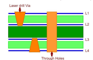
Figure 6: The first step of HDI manufacturing process
2. Stack up of second step HDI PCB.
The second step of HDI manufacturing requires twice the lamination process with blind buried holes. For example, in manufacturing a 6 Layers HDI PCB firstly they need to laminate L2 to L4 layer board, then laser drill L2-L3 or/and L4-L5, and the last finish other processes.
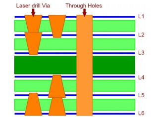
Figure 7: The second step of HDI manufacturing process
3. Stack up of third step HDI PCB with buried via and blind via
The third or fourth step of HDI manufacturing process is similar to the first or second step. The only difference is that it requires more iterations in the lamination process.
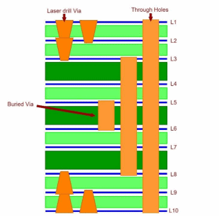
Figure 9: The last step of HDI manufacturing process
- Any layer connection of HDI PCB
In this type of HDI PCB, it requires to manage lamination stackup as normal symmetrical by engineers, but do not ruin the original electronics connection. And its complexity depends on the original design of PCB.
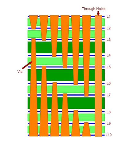
Figure 9: The last step of HDI manufacturing process
HDI PCB Cost
What affects HDI PCB cost? PCBs can be laminated layers of fiberglass (FR-4) with copper coatings etched into traces. And multilayer boards have vias to connect between the layers. In PCB production, it starts with fiberglass material (core or pre-preg) with copper laminated on one or
two sides. Inside layers are coated with photoresist and etched to make bare FR-4 and traces. Then layers are compressed together with the unetched outside layers. After that, the whole PCB is drilled and vias are electrically plated thru. Next, the unetched outside layers are etched. In its
mechanical and chemical process, the mechanical process looks to be a weak point. Drilling is applied in groups (gang drilling) by special drills on granite air tables at 150K – 250K rpm. Most boards are stacked 2 – 3 thicks (4 – 12 boards at once). Drills are exponentially weaker since they
get thinner. There is a constraint related to the drill size/thickness ratio because of this. For this reason, via hole size, which correlates to diameter, and PCB layer count have a prominent PCB price effect. Commonly, PCB cost is affected by these reasons:
(1) Via size; implies HDI/non -HDI decision,
(2) Trace/clearance size; cause yield loss,
(3) Special vias (blind/buried/etc.) cause time and yield, so affects cost,
(4) Layer count; affects cost of materials + yield loss.
Specifically, for HDI PCB manufacture, the characteristics are:
Can have stacked vias (either mechanical or laser)
Affects remarkable cost due to the extra steps (time) needed and equipment cost.
Laser drilled blind vias (<13 mils diameter) on one or more layers, mostly with a throughhole board inserted in between.
If small via sizes (16 mil diameter/8 mil hole size or smaller) are needed, HDI is possibly the only answer. HDI generally reaches the cost of a PCB by 2x, unless the PCB is:
(1) So tiny (e.g. smartphone)
(2) Extremely sophisticated and dense (many devices with large pin count such as an A/V distribution system board in aircraft)
BGAs Affect PCB Cost! Products are commonly planned even before the chips are built. Andcheap consumer electronics are the outcome of heavy competition where the price is their number one concern. For semiconductor companies, to fight in this market they have been concerning lowering system costs. Historically, it implies shrinking die (less component cost and lower power), more integration (less component cost), and shrinking package (expected to be cheaper because of less board space, but now is increasing costs). What they have not done is to know the
PCB cost implications of BGA packages. Now, this becomes the number one topic of customer consideration when discussing new silicon. All of the PCB feature sizes are primarily encouraged by the most sophisticated part on the board, the processor. The processor pitch often defines layers
and design rules (trace/space sizes, laser-drilled vias, blind/stacked vias, via size). This means the BGA ball pitch most often defines PCB cost.
HDI PCB Assembly Process
PCB Assembly with Fine-Pitch. The possibility of a PCB assembly process of fine-pitch (HDI) boards becomes successful can be significantly improved by utilizing some straightforward techniques. In this case, “Fine pitch” boards can be interpreted with boards using an extremely
large number of parts per square millimeters. On the other hand, the parts are significantly close and the rules of the design are forcing the constraints of PCB manufacture tolerances. These aspects are probably also be intended to as “HDI PCB assembly”. PCB design process using
hundreds of parts in a restricted PCB area will be not easy feat that needs many iterations to prevent pitfalls and issues. To make sure our design becomes successful, each step has to be run once.
1. Selecting Part/Component
Firstly, before the process of PCB layout, we have to ensure the selected parts are quite small to have adequate board area during placement. Nevertheless, this process possibly balance board space savings and cost savings. Specifically, the costs raise in assembly process to make
finer-pitch parts placed, particularly components which need certain types of inspection like ICs which need inspection using X-Ray). Figure 10 illustrates a 0.3mm pitch IC. And as a size comparison, there is a penny located near the IC. As tolerances become stricter, cost raises, so
if its priority is reducing cost, then selecting larger parts may become the right method. Most ICs exist in various packages and it is only an issue of exploring its datasheets and scrutinize those things when locating the schematic.
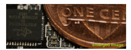
Figure 10: Illustration of PCB Inspection
Another feature to be calculated in high-densities design is the value of each part. A balance should be maintained as well, considering the margin targeted to develop on somethings such as the package dimension of capacitors (which generally depends on power values). For instance, placing a capacitor with 100V value on a PCB with 16V rated capacitor line is not compulsory, and you are commonly willing to provide a sufficient limit of around 20-30% of capacitor voltage values. Nevertheless, the 16V series of this capacitor, which probably is in a tinier size, could reduce it too near and remaining no margin. Therefore, a 25V series capacitor probably is the best choice, optimizing the rating and size of this capacitor and generally the board’s density. A similar thing can be stated for resistors its power (wattage) values. Ensure to choose your parts size properly and constantly scrutinize what type of package you are able to obtain without presenting jeopardy from underrated parts.
2. Size of the Board
Secondly, after the process of design schematic and including all of the parts are determined, is determining a plausible beginning dimension of the board. If then the boards have a “tolerable” dimension and details of the mechanical are still under development, then the procedure could be easier. Specifically, the board dimension will determine the peripheral mechanical hardware, hence group of the mechanical will be on some type of definition process and validation that the desired board dimension even can be obtained. The first action is to examine the possible smallest board. This is commonly done by locating outside connectors, large ICs, and bulky components requiring some rooms near them to separate signals,
remembering the requirement for any susceptible traces and its splitting or isolation in the remain of this board. Occasionally expense can be reduced when selecting preset board shapes/sizes like basic shape of a square which are matched to certain dimensions.
When the preliminary validation has been accomplished, make sure appropriate rules of the design are in location, determined from the capabilities of PCB fabrication in the board vendor. If a desired end-cost requires to be achieved, selecting the optimal right rules of the design in
this point. In this step, the ICs with fine-pitch should be already defined, which may define requirements of the design to some degree. For instance, when a BGA part with ball pitch around 0.4mm is utilized, you will be required to ensure that this specification ends up within the abilities. When ICs with high-speed spec that need impedance control and differential pairs are arranged on being utilized, they will require to be validated by the PCB vendor. When a connector needs multiple odd-shaped places, it may end up into a “adjustable” capability.
3. Placement of Part/Component
When rules of the design are in locations and its capabilities are known, the part placement can start – matching parts close together but with sufficient space for vias, planes, traces, etc. Although this ends up mostly repeated iterations, beginning with high-speed and high-power parts firstly is a great approach, including other mechanical parts. Once these parts are located, it builds a composition from which we work. Things are remarkably strict in this point hence the silkscreen must be restricted to just part outlines and orientation of pin, with no designators reference utilized. It is a normal way that keeps board space, since those designators are greatly only helpful in maintenance or development, and these are not compulsory during assembly. For the placement stage, the board increased a tad in either X or Y. Then it will possibly keep on changing more at this point since parts get routed. Additional reasonings for board areaoptimization in designs with fine-pitch are:
– Decoupling capacitors. Mostly, these types of parts are located directly below, above, or around susceptible pins. And of course placement is quite important.
– Pads Via. This is commonly suggested by the manufacturers of PCB assembly, however can really relieve a little area for traces located in between strictly spaced components.
– Holes of tooling. It is another non-compulsory but helpful supplement to the assembly PCB as well as testing PCB. Tooling holes assist with PCB arrangement for drilling holes, solder stencils, pick n’ place machines, and also test fixtures (if it is necessary).
– Fiducial marks. Putting these small guide markers used for sytems of imaging enable thepick n’ place machine for identifying the PCB location.
There is a balance (almost always) between complexity and cost when we discussing PCB manufacture and assembly, including understanding its trade-offs which could reduce the cost and time in the production, and also development, of a certain product.
