What is multilayer PCB?
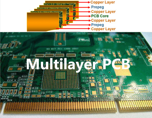
Multilayer PCBs are necessary piece of a large portion of the hardware with regards to interfacing number of electronic parts on the PCB. Multilayer PCB encourages us disposing of the old methods of joining parts where parts were combined by start to finish wiring, brought about covering more weight and space and incapable to satisfy the prerequisites of more sophisticated design. Specialists are in consistent effort to enhance design of electronics with reduced shape hence it gives better client experience and ends up being less expensive than its antecedents. Currently, you have an unmistakable thought for what reason do we want PCB. There are as of now various sorts of PCB board accessible in market for example 1-layer PCB and 2-layer PCB. Yet, now and again these PCBs neglect to convey more sophisticated design due to accessibility of less conductive layers in PCB. Technology is advancing with the more prominent need of creating cheaper gadgets and able to perform a bigger number of capacities than utilizing traditional methods of creating electronic gadgets
Multilayer PCBs became an integral factor with the expectation of developing more conductive layers in PCB than 1-layer or 2-layer boards. The Multilayer PCBs accompany a blend of 1-layer or 2-layer PCB and provide chance to interface more electronic parts in the less space. These PCBs are created from some conductive layers, including protected material amongst them. Multilayer PCBs are generally manufactured in rigid structure, since creating multilayer PCB in flexible structure is hard to accomplish and it additionally brings about more expense than rigid PCBs. Rather than utilizing flexible multilayer PCBs, the greater part of the experts favor utilizing mixes of 1 or 2 sided board which are powerful in a large portion of applications and are less expensive than multi flex boards.
Multilayer boards could be produced with odd/even conductive layers on them. But it is prescribed to utilize multilayer PCB using even layers since it brings about straightforward design and also helps in combining number of various parts on the PCB where design of the board using odd layers could be exorbitant and relates to sophisticated design, creating it hard to combine some electronic parts on the PCB. Additionally, design using odd layers causes it exceptionally troublesome winding the board amongst execution of the project, since odd layer is not similarly disseminated over the entire board structure that could harm the PCBs if they are liable to under hefty loads. Some multilayer PCBs are fabricated so intently, causing it exceptionally troublesome of you to check the absolute layers amount with bare eyes. But you can still figure complete layers amount dependent on layers example and how it is overlaid on the PCB. A various conductive layers amount in the multilayer PCBs could be named as signal, ground or power planes. Ground or power planes are legitimately relative to the quantity of voltage prerequisites on the PCB, if there are some needs of above voltage supply in the board, at that point multilayer boards accompany more than 1 ground or power planes.
Advantages of Multilayer PCB
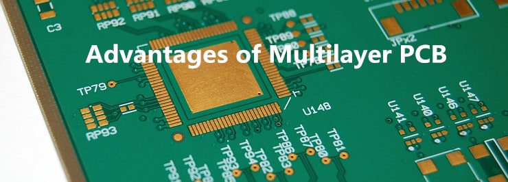
From perspective of technical purposes, multilayer circuit boards provide some advantages in electronic design. These advantages of the multilayer PCBs are including:
- More Effective and Powerful. Multilayer circuit boards are incredibly high-thickness assemblies, joining multi-layers into a one PCB.These close-quarters empower PCBs become more connective, also their natural electrical properties permit them to accomplish more prominent limit and speed regardless of their littler size.
- Improved Durability. Multilayer circuit boards will in general be sturdy by their inclination. Not only implement these multilayer circuit boards need to keep their own weight, yet they should likewise have the option to deal with the warmth and constrain used to tie them together. In addition of these variables, multilayer PCBs utilize multi-layers of protection between circuit-layers, restricting everything along with prepreg holding agent and also protective materials.
- High-Quality Boards. Because of the measure of work plus arranging that have to continue into the making of multilayer circuit boards, these sorts of PCBs will in general be preferred in quality over single and 2-layer PCBs. They likewise will in general be more solid subsequently.
- Smaller Size. The most unmistakable and commended advantages of utilizing multilayer PCBs resides in the size. Due to the layered design, the multilayer circuit boards are naturally littler than different PCBs with comparable usefulness. This provides a significant advantage to current hardware, since the current pattern is moving in the direction of littler, more conservative but more remarkable devices like cell phones, tablets, laptops, and wearables.
- • Lightweight Structure. With smaller circuit boards turns less weight, particularly as the different connectors needed to interlink split one and two-layered PCBs are wiped out for a multi-layered design. This, once more, is useful for current hardware, which are intended more for versatility.
- Not Using Multiple Connection Point. Multilayer circuit boards are intended to fill in as a solitary unit, instead of couple with other electronic circuit parts. Accordingly, they have a single-connection point, instead of multiple-connection points needed toward utilize numerous one-layer PCBs. This ends up being an advantage in electronic item configuration too since they just need to incorporate a single-connection point in last item. This is especially valuable for little hardware and devices designed to limit weight and size.
- Enabled Flexibility. In spite of the fact that this doesn’t matter to all of the multilayer circuit board assemblies, some utilization flexible development procedures, bringing about a flex multilayer circuit board. This could be a profoundly attractive characteristic for applications that mild flexing and bending may happen on a semi-normal premise. Once more, this doesn’t have any significant bearing to all of the multilayer circuit boards, and the more layers joined into a flexible PCB, the less flexible PCB becomes.
Designing Multilayer PCB
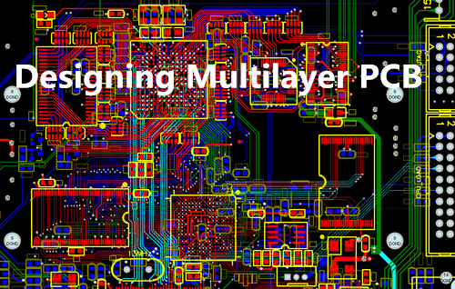
Some of devices in the current modern technology utilize the benefits of using multilayer PCBs. Some of the real employment of multilayer PCBs using complicated layers in which each of these has its own circuit electronics pathways. These are wrapped up to be embedded into a various sophisticated technology like wearable technology, televisions, smartphones, and many medical equipments or devices. If you are looking to make a multilayer circuit board at first time, these are some points you need to consider before designing multilayer PCB. In this part, you will learn 5 tips for designing an optimum multilayer circuit board for your electronic design and other purposes.
1: USE PCB DESIGN SOFTWARE TO SPECIFY LAYOUTS
Single-layer PCBs are remarkable to multilayer design boards. They do not need stacking or layering. Nevertheless, this point is clearly significant in the production of a working multilayer PCB. Yet, why? Because multilayer circuit boards will have various circuits which will deliver energy currents all through the board in order to perform capacities for the innovation it is within. A great deal of energy implies a ton of heat! It can make some issues if not took care of accurately in design process. Utilizing a PCB software could assist you with deciding the most ideal approach to design your board to prevent from overheating and also electronic noise problems correlated to multilayer PCBs.
2: SELECT THE CORRECT BOARD SIZE
While thinking about how to make the optimum multilayer PCB design, you should ensure that you pick the correct size of the board for your purpose. Your board size will affect the electronic circuit design just as the different parts that you should utilize. Likewise, 1 layer of the multilayer circuit board will probably have more or fewer circuit pathways comparing to another layer.
3: SELECT THE CORRECT MATERIALS
Just like design of whatever else, materials that you are using will be different upon the method in which the products are utilized. In multilayer PCBs case, there are various alternatives with regards to materials that you can utilize in manufacture process. Particularly, in fact that multilayer PCBs have to be carefully planned considering electrical stability. Perhaps one of good materials utilized for the manufacturing of multilayer circuit boards is PTFE (polytetrafluoroethylene). This kind of material is picked because of its constant of low dielectric and also its low-loss properties. This implies it can undoubtedly adjust with varying and changing temperatures.
4: OPTIMIZE PRODUCTION PROCESS OF THE BOARDS
Production is progressively significant. Production issues can cause any problems which can deliver the innovation pointless. Thus, you need to ensure that your production cycle is prepared appropriately to deal with the production of multilayer PCBs. The layers stackup, etching of the board, drilling and lamination process, and also the testing cycles will be distinctive while making multilayer PCBs.
5: CONSIDER YOUR LAYERS STACKUP
Making a powerful multilayer circuit board is the means by which you decide your layers stackup. Contiguous signal layers ought to be routed oppositely, horizontally or vertically. Routing them along these lines can diminish the probability of cross-communication problems. Furthermore, routing signals a similar way will deliver a huge amount of energy aside or one territory of the multilayer PCB. This can bring about overheating and also make the board pointless.
Recommended Stackup for Multilayer PCB
Planning for configuration of the multilayer PCB stackup is an important points to achieve the best performance of a device board. An appropriate substrate of PCB stackup can effectively decrease crosstalk, electromagnetic emissions, and enhance the board signal integrity. A bad stackup PCB can add crosstalk, emissions, and also the product becomes more vulnerable to external noise. These problems can affect intermittent running because of the glitches of timing and interference significantly decreasing performance of the board and its reliability.In multilayer PCB, plane provides dramatic decrease in emission over 2-layer boards. Empirically, a 4-layer board will result less radiation (15-db) comparing to a 2-layer board. The boards that contain planes enable signals become routed in microstrip/stripline configurations of line of impedance transmission that can be controlled making less radiation comparing to the random traces on top of a 2-layer PCB.The signals in the board are strictly coupled to planes, either power or ground, decreasing crosstalk and also enhancing signal integrity. Power and ground planes in a high-speed systems show three critical functions:
- Distribute power (low inductance) to logic devices
- Give stable ref. voltage for sharing digital signals
- Controls crosstalk amongst signals
When choosing a multilayer PCB stackup we should concern the following:
- Coupled signal layers (<10 MIL) to their close planes
- A signal layer should always be adjacent to a plane
- A ground or power plane can be utilized for signal return path
- Define the signal return path.
Now, let’s take a look at the most common configurations of multilayer PCB:
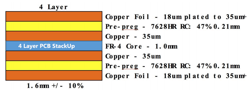
Pic1: 4 Layer PCB StackUp
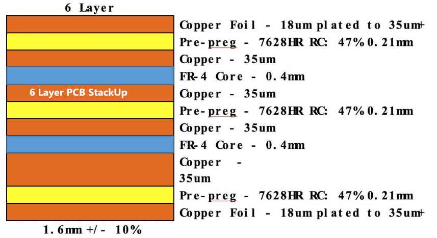
Pic2:6 Layer PCB StackUp
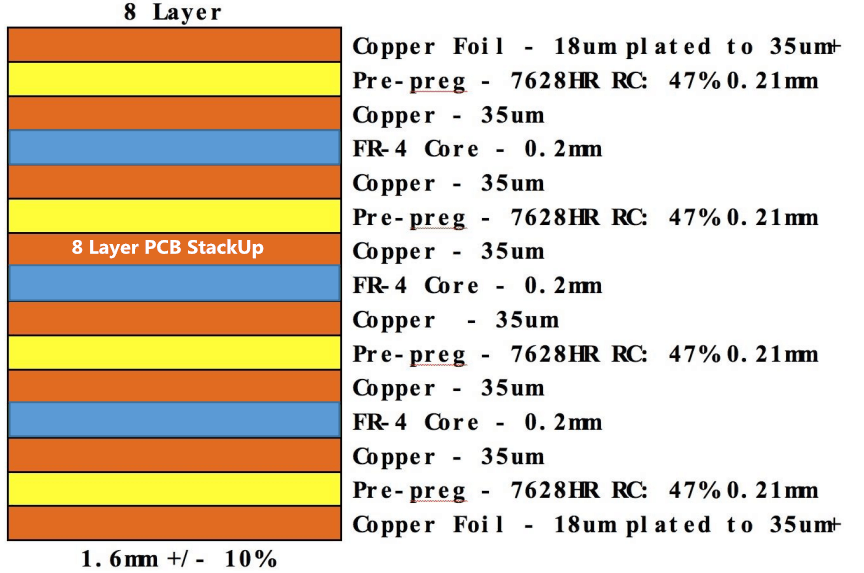
Pic3:8 Layer PCB StackUp
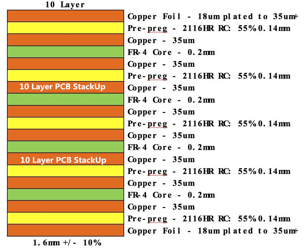
Pic4:10 Layer PCB StackUp
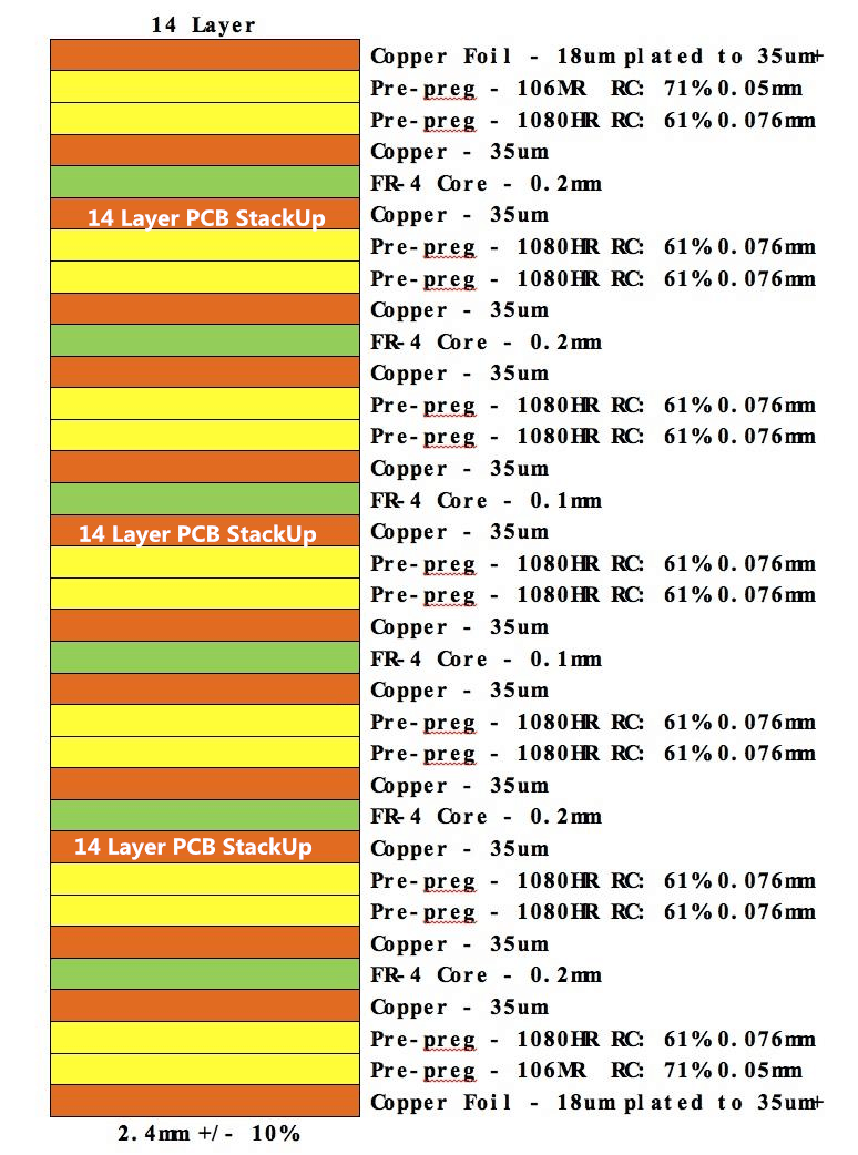
Pic5:14 Layer PCB StackUp
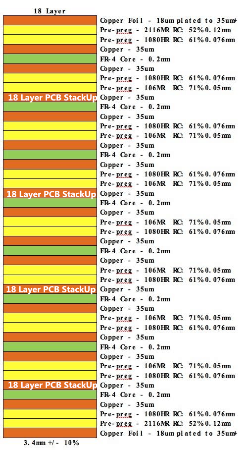
Pic6:18 Layer PCB StackUp
Multlayer Pcb Manufacturing
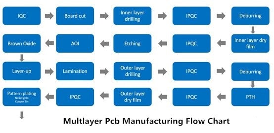
Front-end of the engineering part. This is an initial step to creating PCBs. Amongst this step, the maker will deal with circuit board designs to start arrangements for manufacturing. There are various ways to deal with this cycle, however it fundamentally involves creating step-by-step directions for manufacturing the circuit board. All of the designs are assessed and the organizer likewise makes the “cycle card”, that will be shifted with the circuit board all through its designing cycle. The CAM designer will likewise play out a thorough design audit and afterward convert all records into the information format needed for assembling. Front-end of the engineering part is all the more a planning stage where the organizer surveys all the prerequisites and data introduced for the manufacturing of the circuit board. This incorporates buy request details, special instructions, manufacture drawings, due dates and quantities just as materials. Moreover, the CAM engineers are entrusted with playing out a review of in-depth data and decides the tooling needed to accomplish the final manufacture product. Lastly, engineers for the most part follow a point by point list that incorporates:
- Data cleanup. Involves stacking the information into the CAM programming to perform information cleanup and altering, for example, doling out names and layer arrangement.
- Drill information confirmation. This guarantees the gap size include matches in the information document matches what is in the manufacture. It additionally checks uncommon steering, patterns and plating necessities.
- PCB editting. Here, enginner will runs the DRC to audit picture documents and make helpful changes. It might incorporate resizing the drill size, altering layers, including BAC markings and including scratch pay.
- Panelization. depend on perfect match, the boards are placed on production panel by using tooling, labels, and borders. In light of the ideal fit, the board is spread out on the creation board utilizing tooling, outskirts, and names.
- Outputs. It is the last advance of front-end producing and includes creating various yields, including drill documents AOI defeat records and picture records.
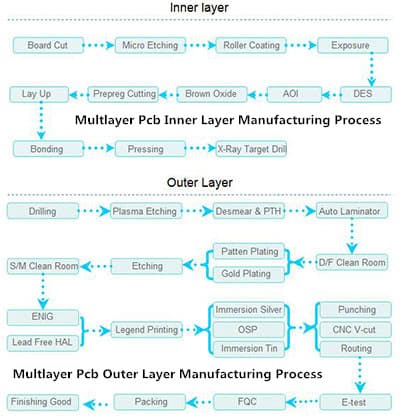
The way toward creating multilayer PCBs. A few elements go into delivering top notch multilayer PCBs. The cycle includes explicit advances important to guarantee each perspective is secured. Since there are various kinds of multilayer sheets, the assembling cycle might be diverse dependent on the exceptional plan you need to accomplish. Other than front end arranging, the overall method includes:
- Photo plotting. Changes over the photograph information and changes over it to picture pixel.
- Imaging plus DES. DES stands for develop, etch, and strip. In this step, it implements the essential picture on PCB.
- Automated optical examination. Investigates the layers of the multiplayer PCB before overlay.
- Oxide lamination and treatment. chemical treatment implemented on the internal layers of the PCB. Overlay ties the various layers of copper and fiberglass together.
- 5. Drilling and also electroless-copper deposition. In this cycle makes the necessary drill openings and channels on the PCB. They are then secured by copper stores.
Fabrication, Electrical test, micro-sectioning, final inspection. Makers may likewise incorporate different cycles to accomplish one of a kind plans and particulars. Each progression has a one of a kind cycle that can be altered by the creation necessities. Producers can likewise utilize various innovations in various stages. For example, some utilization movie plotting during the photograph plotting measure, while other uncommon LDI or laser-direct-imaging. Review is likewise the way in to any multilayer PCB. They help to guarantee the board is practical and meets client particulars.
Summary. Creating multilayer circuit boards is a long cycle on paper. Front-end producing normally takes the longest time and the maker utilizes this stage to guarantee all prerequisites, tooling and measurements are all together. Likewise, a few tests are directed to investigate and distinguish any mistakes in the plan. In the event that you are involving in the business for multilayer circuit boards (PCB), it is suggested to pick high-quality and experienced board makers to guarantee premium quality items. It is additionally basic to enlist proficient CAM designs that can convey remarkable answers for your necessities.
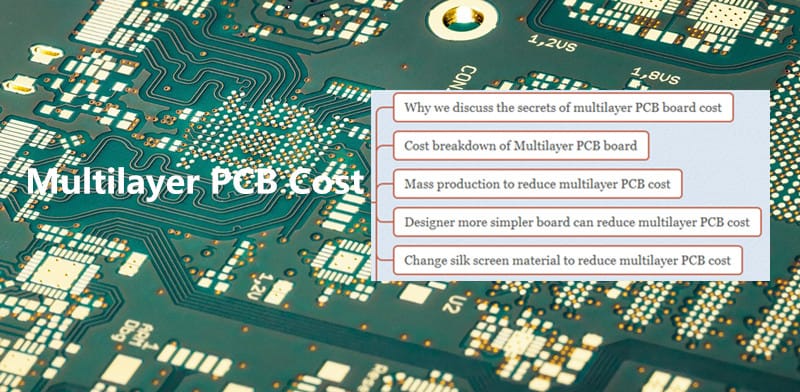
How To Save Multilayer PCB Cost
Multilayer PCB Cost per Layer. Single layer PCBs ordinarily include: a keep-out layer, a mechanical-layer, an overlay-layer, a solder-paste layer, a routing-layer, and a solder-mask layer. Multilayer PCBs include those similar layers just as a blend of extra ground planes, power planes, and all the more routing-layers. The most recent innovation of PCBs is multilayer innovation. These PCBs are fabricated on models for different applications, from two, four to six multilayer PCBs. When your company relies upon the most recent innovation, it is advantageous to get the most recent applications on the PCB. Multilayer circuit board is viewed as the most recent innovation of PCB. In the event that you would prefer not to pay a high expenses or countless requests in the long run however prefer SME searching for the most recent innovation in these items, can search for companies which give PCBs at sensible costs. Notwithstanding giving this innovation to SME, companies which make multilayer PCBs are also able to support business visionaries. Since these companies/vendors mass produce PCBs, the conventional PCB idea permits business people to get the applications that they need on their models to address the issues of their items.
There are a few positive perspectives while picking a company which concerns around structuring multilayer PCBs for SMEs. Most importantly, the amount you have to purchase should not as much as that from a huge manufacturer. Furthermore, you can obtain models structured by your particular requirements, picking your accomplice companies to guarantee that you obtain the items and cause it run easily. Utilizing makers that make multi-layer PCBs for SMEs can furnish you with the following best item created by bare-hand without spending the expense of hand-made items. By utilizing a company which produces multilayer PCBs for SME, your business can acquire innovative multilayer circuit boards with quick conveyance times and reasonable expenses.
Reducing Multilayer PCB Cost. When structuring PCBs, tight resistances ought to be kept up on the PCB as well as in your wallet. Now we will provide 13 realistic and creative approaches to decrease your general flex PCB fabricating costs. These recommendations can be implemented to even six layer flexible PCBs.
Reducing Circuit Costs
The way where an electronic circuit is planned on a board directly affects your expense. This could be diminished somewhat with the assistance of a couple of savvy planning methods:
- Suggested tolerances ought to be carefully adhered to.
- Expose your electronic circuit. One large electronic circuit will charge you more expenses. A series of smaller electronic circuitry is the best approach.
- Unbounded zones ought to be kept to a min. space
Other Design Requirements
- If our design allows it, think about structure a PCB with less layers. You should consider assembly costs and application requirements.
- It is more affordable to make a PCB with even-layers instead of odd-layers.
- Round thru-holes, when contrasted with opened or the square ones diminish the general expense and time.
- Vias which are buried or blind eventually costing more.
- The lower spacing and width of conductors, expense will become higher.
- The generally speaking PCB expenses can be decreased radically by assembling them in mass amounts.
- Relaxed tolerances charge less contrasted with tight tolerances.
- Maintaining similar stiffeners thickness all through the circuit board will help decrease costs.
- Choose for stiffeners instead of utilizing rigid-flex PCBs, that are more costly.
- Make sure that your circuit board layout is in ideal condition at the designing step. Incorrect design will demolish the circuit board and increment your expenses.
All the previously mentioned expense-saving strategies will be different as per the application. In some cases, the cash saved in parting an electronic circuitry or layers of a console can mean higher PCB assembly expenses. Each circumstance is special and ought to be managed likewise. Talk about your requirements with a maker to comprehend the consequences of each corner-cutting method.
