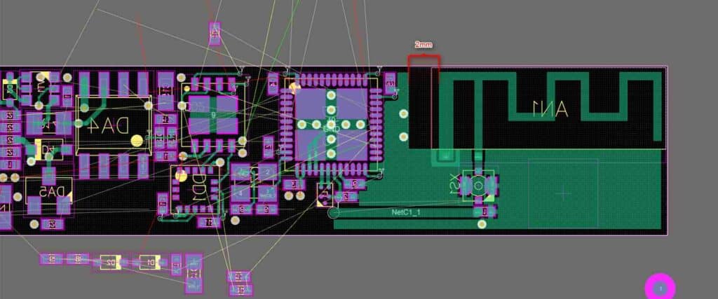
Delay layout is a critical aspect of designing electronic circuits that involve time-sensitive signals. It involves the careful consideration of signal propagation time, signal distortion, and noise. Delay layout is particularly important in high-speed electronic circuits, where even small delays can result in significant signal degradation.
To achieve optimal delay layout, designers must pay close attention to the physical layout of the circuit, the placement of components, and the routing of signals. This involves a deep understanding of both the electrical and physical properties of the components used in the circuit.
In this article, we will explore the fundamentals of delay layout and provide practical tips and strategies for achieving optimal signal timing in electronic circuits. Whether you are a seasoned electronics designer or a beginner, this article will provide valuable insights into the critical role of delay layout in electronic circuit design.
Reasons for Delay Layout
Delay layout is an important aspect of circuit design that helps to optimize the performance of electronic devices. Here are some reasons why delay layout is necessary:
-
Signal Propagation Delay: In an electronic circuit, the signal propagation delay is the time taken for a signal to travel from one point to another. Delay layout helps to minimize this delay by optimizing the routing of signals and reducing the distance that signals need to travel.
-
Clock Skew: Clock skew is the difference in arrival times of clock signals at different points in a circuit. Delay layout helps to minimize clock skew by ensuring that clock signals arrive at different points in the circuit at the same time.
-
Power Consumption: Delay layout can also help to reduce power consumption in electronic devices. By optimizing the routing of signals, delay layout can reduce the capacitance and resistance of the circuit, which in turn reduces power consumption.
-
Timing Constraints: Electronic devices have timing constraints that must be met for them to function properly. Delay layout helps to ensure that these timing constraints are met by optimizing the routing of signals and reducing the signal propagation delay.
In conclusion, delay layout is an essential aspect of circuit design that helps to optimize the performance of electronic devices. By minimizing signal propagation delay, reducing clock skew, reducing power consumption, and meeting timing constraints, delay layout ensures that electronic devices function properly and efficiently.
Impacts of Delay Layout

Delay layout is a crucial aspect of designing integrated circuits (ICs) that affect the performance of the entire system. It refers to the process of introducing intentional delays in the signal path to ensure that all the signals arrive at the same time. Here are some of the impacts of delay layout:
-
Timing Violations: Delay layout is used to ensure that all the signals arrive at the same time. If the delay is not appropriately designed, it can lead to timing violations, which can cause the system to malfunction.
-
Power Consumption: Delay layout can significantly impact the power consumption of the system. If the delay is too high, it can lead to increased power consumption, which can reduce the battery life of the device.
-
Signal Integrity: Delay layout can affect the signal integrity of the system. If the delay is not appropriately designed, it can lead to signal distortion, which can cause errors in the system.
-
Area Utilization: Delay layout can impact the area utilization of the system. If the delay is too high, it can lead to increased area utilization, which can increase the cost of the system.
In conclusion, delay layout is a crucial aspect of designing integrated circuits that can significantly impact the performance of the system. It is essential to ensure that the delay is appropriately designed to avoid timing violations, reduce power consumption, maintain signal integrity, and optimize area utilization.
Strategies to Avoid Delay Layout

Delay layout can be a time-consuming and frustrating process, but there are strategies you can use to avoid it. Here are a few tips to help you streamline your design process and avoid the need for delay layout:
-
Plan ahead: One of the most effective ways to avoid delay layout is to plan your design ahead of time. This means thinking through your design and making sure that everything fits together properly before you start laying out your components. By doing this, you can avoid having to make last-minute adjustments that can cause delays.
-
Use standardized components: Another way to avoid delay layout is to use standardized components whenever possible. This means using components that are pre-designed and pre-tested, so you don’t have to spend time designing and testing them yourself. By using standardized components, you can reduce the risk of errors and save time in the layout process.
-
Keep it simple: When designing your components, try to keep them as simple as possible. This means avoiding unnecessary features or complexity that can make it harder to lay out your components. By keeping things simple, you can reduce the risk of errors and make it easier to lay out your components.
-
Test early and often: Finally, it’s important to test your components early and often. This means testing your design as you go along, rather than waiting until the end of the process. By doing this, you can catch errors and make adjustments before they become bigger problems that require delay layout.
By following these strategies, you can streamline your design process and avoid the need for delay layout. With a little planning and attention to detail, you can create designs that are efficient, effective, and easy to lay out.
Mitigation of Delay Layout
Delay layout is a common problem in the design of integrated circuits. It is caused by the time it takes for a signal to travel from one point to another on a chip. Delay layout can cause timing errors, which can result in the failure of the circuit. Fortunately, there are several ways to mitigate the effects of delay layout.
Routing
One of the most effective ways to mitigate delay layout is through careful routing. Routing is the process of connecting the various components of a circuit. By carefully routing the signals, it is possible to minimize the distance that the signals have to travel. This can help to reduce the delay and improve the overall performance of the circuit.
Timing Analysis
Another way to mitigate the effects of delay layout is through timing analysis. Timing analysis is the process of analyzing the timing of a circuit to identify potential issues. By identifying potential timing issues early in the design process, it is possible to make changes to the layout to mitigate the effects of delay layout.
Clock Distribution
Clock distribution is another area where delay layout can be mitigated. Clock distribution is the process of distributing a clock signal to various components of a circuit. By carefully designing the clock distribution network, it is possible to minimize the delay and improve the overall performance of the circuit.
Buffering
Buffering is another technique that can be used to mitigate the effects of delay layout. Buffers are components that are used to amplify signals. By adding buffers to the circuit, it is possible to reduce the delay and improve the overall performance of the circuit.
Overall, there are several ways to mitigate the effects of delay layout in integrated circuits. By carefully designing the layout, performing timing analysis, and using buffering and clock distribution techniques, it is possible to minimize the delay and improve the overall performance of the circuit.
