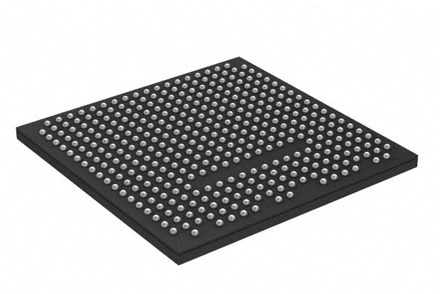
LFE5UM-85F-8BG381C belongs to the ECP5 family of Field Programmable Gate Arrays (FPGAs). Lattice Semiconductor manufactures it. This FPGA is known for the design optimizations, making it ideal for high-powered applications.
LFE5UM-85F-8BG381C supports a wide range of high-performance features, including but not limited to the following:
- High-speed SERDES
- Enhanced DSP architecture
- High-speed source synchronous interfaces
High-Performance Delivery
At the core of LFE5UM-85F-8BG381C’s performance is the combination of several high-performance deliverable features. From the high-speed source synchronous interfaces to the high-speed SERDES; these features go hand-in-hand to increase this FPGA’s performance.
The most remarkable thing about the high-performance features is the fitting into an economical FPGA fabric.
Now, we are going to discuss some of the additional features we like about this FPGA.
Multi-Interface Support
LFE5UM-85F-8BG381C supports a wide range of interfaces, through the pre-engineered source synchronous logic implemented in it. This implementation paves the way for the FPGA to support several interfaces, examples being:
- 7:1 LVDS
- DDR2/3
- XGMII
- LPDDR2/3
Performance Meets Cost-Sensitivity
LFE5UM-85F-8BG381C does not just stop at improving the performance of the device. It also makes sure that the cost implications are considered too.
The FPGA balances the high-performance with low-cost and high-volume applications through the combined use of the nm technology, and an advanced FPGA device architecture.
Device Migration
Migrating or moving a circuit board design from the original board to another hasn’t been as hassle-free as LFE5UM-85F-8BG381C makes it to be.
The design interoperability is derived from the pin-to-pin compatibility of the ECP-5G family with the ECPUM devices. The compatibility makes LFE5UM-85F-8BG381C and other related ECP-5 FPGA devices to enable design porting from the former to the EPC5UM devices and vice-versa.
Multi-Data Protocols Support
Rest assured that different kind of data protocols are supported with the LFE5UM-85F-8BG381C FPGA. The multiple data protocol support is enabled by the high-speed SERDES, which has a set of dedicated Physical Coding Sublayer (PCS) functions.
The major multiple data support is enabled through the low-transmit jitter and the high-jitter tolerance. These two jitters allow passage for the SERDES and the PCS functions to be further configured or optimized to support several data protocols.
Some of the supported data protocols are:
- CPRI
- PCI Express (PCIe)
- Ethernet-related data protocols, such as SGMII, XAUI, and GbE
LFE5UM-85F-8BG381C Supports Flexible Configurations

LFE5UM-85F-8BG381C offers a variety of device configuration options, ranging from the Slave SPI, Shared bank for Configuration I/O, TransfFRTM I/O, which is used for the simple field updates.
LFE5UM-85F-8BG381C also supports SPI boot flash and dual-boot images.
System-Level Handling Functions
To ensure an excellent handling of the device, LFE5UM-85F-8BG381C has been able to delegate a wide range of functions. These functions are generally called the Single Event Upset (SEU) Mitigation Support.
The support rendered here is to prevent the device from malfunctioning due to a single or one fault.
Here are some of the SEU mitigation supports rendered here:
1. Soft Error Injection
The function of this SEU is to emulate the SEU event in view, with the goal of debugging the system error handling.
2. Soft Error Correction
This works together with the Soft Error Detect, whereby the former detects the errors, while the Soft Error Correction fixes the errors. It does this without usurping or stopping the active user operation.
LFE5UM-85F-8BG381C FPGA Attributes
The table below represents the values of the different properties for the LFE5UM-85F-8BG381C ECP5 FPAG device.
| Attributes | Description |
| Mounting Style | Surface-mount |
| Number of Logic Cells/Elements | 84,000 |
| Base Product Number | LFE5UM-85 |
| Number of CLBs/LABs | 21,000 |
| Operating Temperature | 0˚C to 85˚C |
| Total RAM Bits | 3,833,856 |
| Package/Case | 381-FBGA |
| Number of I/O Pins | 205 |
| Series | ECP5 |
| Voltage – Supply | Between 1.045 volts and 1.155 volts |
The ECP5/ECP5-5G Design Iteration
As one of the devices under the ECP5/ECP5-5G FPGAs, LFE5UM-85F-8BG381C is also optimized for high-performance, cost-optimization and accelerating both device connection and operations.
Here are some major features of this FPGA family:
Improved Routing Architecture
To ensure an even flow or distribution of the data, LFE5UM-85F-8BG381C uses an improved routing architecture. It includes an advanced FPGA device structure and an enhanced DSP architecture.
The improved architecture, combined with the dual-channel SERDES and the enhanced DSP blocks provide LFE5UM-85F-8BG381C with up to 4x improved multiplier utilization.
Programmable I/O
LFE5UM-85F-8BG381C’s Input and Output (I/O) pins are configurable. The configurations extend to the following:
- MIPI D-PHY input/output interfaces.
- LVCMOS 33/25/18/15/12
- LVVTL
- LVPECL
- XGMII
- 7:1 LVDS
- LVDS
- Bus-LVDS
Low-Power Consumption
LFE5UM-85F-8BG381C offers a lower-power consumption – which could be up to 30% reduced power.
The lower-power usage is powered by the quad-channel SERDES that function below 0.5 watts; and the single-channel SERDES that functions below 0.25 watts.
High-Speed
LFE5UM-85F-8BG381C’s higher-performance is enabled through the 3.2 Gbps SERDES rate with ECP5, and which can potentially reach up to 5 Gbps with the ECP5-5G.
LFE5UM-85F-8BG381C Supports Small Form-Factor Packages
LFE5UM-85F-8BG381C is one of the FPGA devices ideal for use with the applications, requiring a smaller package. The small form-factor package design is via the support for up to 85,000 Look-up Tables (LUTs). These LUTs are packaged in 10 by 10 mm, in a 0.5 mm pitch package. It is also compatible with SERDES.
One unique attribute of the small form-factor design is the “smart ball depopulation”; a concept that simplifies the integration of the package/case with the low-cost Printed Circuit Board (PCB) technology.
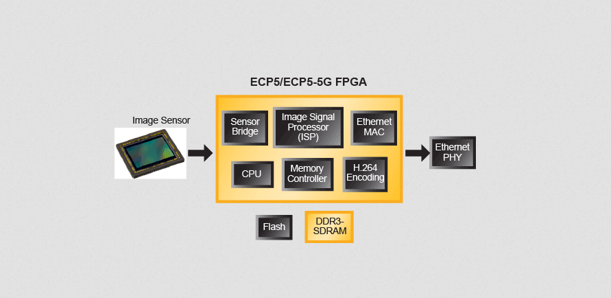
The low-cost packages are small-sized, help in “twisting” the functional density and are ideal for implementing connectivity, imaging and video functionality in high-volume applications.
Examples of the supported applications are:
- Industrial video games
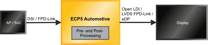
- Automotive devices
- Broadband access equipment
- PCIe Side-Band Solution for Microservers
- It is also ideal for the Small Cell Wireless Base Stations
Supported Operation Methods
LFE5UM-85F-8BG381C supports up to four (4) modes of operations; namely: Ripple Mode, Logic Mode, ROM Mode and RAM Mode.
The RAM Mode is used to facilitate the distributed memory initialization, especially through the Slice 2 LUT block to provide control signals and memory access.
While the ROM Mode enables preloading completion through the programming interface while in the PFU configuration; the Logic Mode works by allowing the configurations of the Look-Up Tables (LUTs) via a 4-input combinatorial LUT.
The Ripple Mode allows the implementation of specific (small) arithmetic functions, such as the (up and down) counter 2-bit, and the multiplier support.
Final Words
LFE5UM-85F-8BG381C is an FPGA device, enabling the real-time configuration of relevant elements, while allowing for flexibility in the process of doing that.
