What is FPGA
A field-programmable gate array is abbreviated as FPGA and it is one of the popular programmable circuits. It is an integrated circuit (IC) that can flexibly be programmed according to the requirements. FPGA is made up of modular integrated circuits, some of those modules consist of sequential components such as the flip-flops which are the smallest memory element of FPGA, whereas other modules function as combinational components such as multiplexers and logic gates.
FPGA Building Blocks
FPGAs contain logic blocks as well as input and output blocks. These input/output blocks are also called interconnect resources. We can get various kinds of digital circuits by reconfiguration of logic blocks and interconnect resources. FPGAs are built using programmable logic devices (PLDs) also called configurable logic blocks (CLBs). A CLB may further contain different logic elements such as flip-flops and lookup tables (LUTs). FPGAs consists of thousands of these blocks. They can implement complex logic functions and solve any computable problem.
Parallelism
The distinct property of FPGAs is the support for parallelism. Distinct blocks can process tasks independently. This parallel processing results in speedier computations and more efficient performance because one block does not affect the other blocks. The parallelism becomes essential when data arrives at a faster rate than it can be processed. More blocks of FPGA can be used to simultaneously process the data instead of slowing down the data arrival rate. For example, your FPGA receives data at 100kB/sec rate and the data is arriving in 10kB blocks. You can configure the input block to distribute the coming data across 10 CLBs to process it without any lag.
Types of FPGA
There are FPGAs that can be programmed once, but the more popular are reprogrammable FPGAs. FPGAs are categorized by their method of storing configuration data. The functionality of an FPGA is designed according to the configuration data it is going to be processing. FPGA has the following three configuration types.
Anti-fuse Based
In a fuse or Anti-fuse FPGA, the Anti-fuse element is responsible for the processing of configuration data. We can program this type of FPGA only once; this process is permanent. This type of device starts as an open circuit, hence the name fuse, however once programmed they act as a short circuit, hence the name anti-fuse.
SRAM Based
We can program SRAM FPGA multiple times. The exact number of reprogramming depends on the requirement of the algorithm and the model of FPGA. In this type, configuration data can be stored in static memory cells (SRAM). Static memory consists of an array of latches. SRAM is a volatile memory and it loses data if power is cut off. Therefore, they need to be reprogrammed every time they are powered up from an external nonvolatile memory. This requirement of an external nonvolatile memory is solved by the SRAM-based FPGAs that have built-in flash memory blocks.
Flash Based
In built-in flash SRAM FPGAs, the flash memory is used once at the power start-up to load configuration data to SRAM. However, in flash-based FPGAs, the configuration data itself is stored in flash memory rather than SRAM. The configuration data is kept stored even after the power is turned off. We can reprogram these types of FPGAs by directly altering the data in the flash.
Popular FPGA Brands
Design of FPGAs is an application-specific process. There are low powered FPGAs that use power in a fraction of a watt. Whereas some midrange models use around one watt and support a diverse range of applications. Then there are other higher power FPGAs that require hundreds of watts energy, they are mostly used for larger applications such as data centres.
According to the report published by Market & Market, the FPGA market size is projected to reach $8.6 billion by 2025 from $5.9 billion in 2020. Main contributing factors for faster growth include greater adoption of Internet of things (IoT) and artificial Intelligence (AI) technologies, and the relative simplicity of FPGA programming. Major FPGA manufacturers are listed below:
Xilinx
It is a well-known programmable device designer and manufacturer. It has the credit of inventing FPGA and fully programmable system-on-chip (SoC). Xilinx has launched an ACAP chip that is specifically designed for AI purposes. It also manufactures system-on-modules (SoM), 3D ICs, and other development tools.
Intel Corporation
In 2015, Intel acquired Altera Corporation and Corporation is one of the largest computing device manufacturers across the world. In December 2015, Intel Corporation acquired Altera Corporation, a top FPGA producer. Intel started producing FPGAs and other programmable devices along with its traditional products such as processors, servers, boards, and chipsets.
Microchip Technology
Microchip Technology is famous for embedded control devices. It started producing FPGAs in 2018 after acquiring US Microsemi. Apart from FPGAs, Microchip manufactures PLGs, amplifiers, security ICs, and data converters among others.
Lattice Semiconductor
It specializes in the manufacturing of low power cost-effective FPGAs along with complex PLDs. These FPGAs can be used for industrial, computing, communications, and medical purposes. Additionally, Lattice Semiconductor provides video connectivity solutions, power control devices, and IP products.
QuickLogic Corporation
QuickLogic is famous for multicore low-powered semiconductor devices. It manufactures industrial IoT products, low-powered SoCs, FPGAs, and eFPGAs. Its FPGAs are specifically designed for machine learning, security and defence, and IoT.
Efinix
Primary product of Efinix is FPGAs. Additionally, it produces integrated development environments. Efinix’s FPGAs feature Quantum technologies, which claim to have four times greater power performance than conventional FPGAs. These quantum FPGAs are ideal for IoT, wireless connectivity, video surveillance, computing, and data storage.
FPGA Prices
The price of FPGAs ranges from few USDs to thousand USDs. It is vital to choose an FPGA that is a proper fit for a certain application. The cost of an FPGA is justified if the application needs a lot of data to be processed in parallel. FPGAs are very good at parallel computations.
The price of an FPGAs depend on various features such as: the quantity in which the FPGAs are being bought, less price is offered by the vendor when more quantity is needed; the number of CLBs, they range from 64 to 316620; number of logic cells, they range from 238 to 5540850; the number of I/O connections, their range is from 34 to 1456; and finally the amount of available RAM.
Xilinx Prices
Least expensive FPGAs of Xilinx spartan series can be bought in around $8. However, a low-end Spartan 6 can be bought in $12, it is capable to run 8-bit CPU. A low-end Spartan 7 is priced at around $22. Similarly, a low-end Artix model is priced at $28 while an Artix 7 is priced at around $35. Different Xilinx models with varying capabilities such as Artix, Spartan II, Spartan 3, Spartan 6, and Spartan 7 are available from few USD to 100 USD. There are FPGAs that cost more than $ 100,000 and they offer maximum FPGA capabilities.
Intel Prices
With minimum specification, intel’s FPGAs are available from $4. Popular models of Intel’s FPGA include Arria, Cyclone, Max, and Stratix. Intel’s Stratix is a high-end FPGA model. It is available in $91,558. Its price depends on the features selected such as amount of RAM, number of logic cells, number of CLBs etc. Stratix series is available from $10,000.
Lattice Semiconductor
Low-end FPGA by Lattice Semiconductor is available from $1.5, it has 48 CLBs, 384 Logic cells, and 21 I/O connections. High-end Virtex Ultra-scale is available in $115,257, it is equipped with 162,960 CLBs, 2,851,800 logic cells, and 624 I/O connections.
Comparison Table
| CLBs | Logic Cells | No. of I/O | No. of Gates | RAM (Bits) | Price ($) | |||
| Xilinx | LOW-END | 176 | 1584 | 68 | 5×10^4 | 55296 | 8.33 | |
| HIGH-END | 162960 | 2851800 | 624 | 74344038 | 115,257 | |||
| Intel | LOW-END | 125 | 2000 | 27 | 110 | 110592 | 2.84 | |
| HIGH-END | 350000 | 2800000 | 296 | 91,558 | ||||
| Lattice Semiconductor | LOW-END | 160 | 1280 | 28 | 65536 | 2.45 | ||
| HIGH-END | 11875 | 95000 | 520 | 5435392 | 592.87 | |||
| Effinix | LOW-END | 3888 | 33 | 78848 | 1.04 | |||
| HIGH-END | 112128 | 278 | 5536768 | 44.73 | ||||
| Microsemi | LOW-END | 34 | 1×10^4 | 3.48 | ||||
| HIGH-END | 440 | 1×10^6 | 202752 | 29,314 | ||||
| Microchip Technology | LOW-END | 256 | 128 | 1×10^4 | 2048 | 14.28 | ||
| HIGH-END | 2304 | 161 | 5×10^4 | 18432 | 112 |
Why are FGPAs Expensive
There are many aspects responsible for the high cost of FPGAs. One is the customers with low volume of needs. These low volume customers require support and services. The price of silicon and the IC wafer and package is also very high. Chips are expensive and the chip area needs to be utilized properly. In FPGAs, the majority of the chip area is used by interconnect resources, interconnect resources connect logic blocks with programmable I/O connection blocks. Faulty wafer is also a common problem and in larger chips the probability of faulty wafer increases. There are also costs of processing silicon wafers for chip production. Another factor for the high cost of FPGAs is the individual testing. This testing is done to make sure that the millions of interconnects between logic blocks are functioning properly.
FPGA Applications
FPGAs are reusable because we can program them several times. The reusability makes highly functional and suitable for many applications. FPGAs with its internal memory and a large set of multipliers are suitable for signal processing such as multiplexing and signal conditioning.
With arm-based FPGAs, SoCs can be created to carry out tasks such as hardware acceleration. FPGA based highly customizable SoCs are commonly used for data center and network security hardware. Other applications of FPGAs include: video and image processing and manipulation, wireless communication, instrumentation, and medical applications such as MRI, CT-Scan, and ultrasound, etc.
FPGAs are suitable for machine learning, compression, and image recognition. FPGAs can be used in the process of developing Application Specific Integrated Circuits (ASICs) such as ASIC emulation and verification. Presently, FPGAs are being used in the fields such as aerospace, automotive industry, super computers, financial applications, and cryptocurrencies.
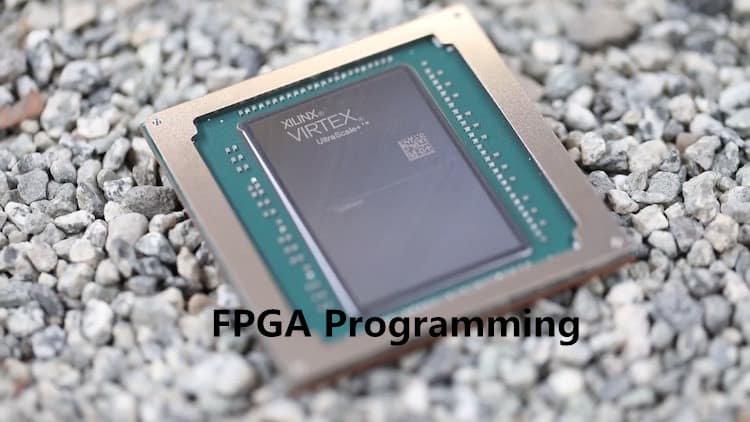
FPGA Programming
FPGA function is established either by schematic design or by using the hardware description language (HDL). It is easier to work with HDL because it enables the developer to specify high level functions in a large application instead of drawing the whole schematic manually. However, the visualization is easier in the schematic method.
A netlist is generated using a specifically developed tool. This netlist is then fitted to the FPGA architecture using the place-and-route method. The results of place and route technique are validated using performance simulation and timing analysis.
After this process, a dedicated software is used to generate a binary file. Each vendor has their own proprietary software. The binary file is essential for the reconfiguration of FPGAs. It is uploaded to the FPGA via a serial communication interface. The interface is usually JTAG, which is the standard for testing design.
Some frequently used HDLs include Verilog and VHDL. Recently, developers are using Open Computing Language (OpenCL) to benefit from the advantages of FPGA. OpenCL is used to design FPGAs in a way that is more power efficient and has greater performance. In OpenCL, the code is written in C and mapped to FPGA using OpenCL functions.
Programming FPGA is a complex process. To take some of the complexity away and speed up the design process, libraries of predefined functions and schematics are available. These libraries are called intellectual property (IP) cores.
IP cores are provided by FPGA manufactures under proprietary licenses. Other third-party providers also sell IP cores. There are other opensource IP core developers, they are community based, and they share open-source hardware for free.
The process of design is carried out in the following order, the developer will simulate the design at multiple stages throughout the design process. First, an RTL description is simulated in HDL. It is done by creating test benchmarks for the simulation of system performance and observing results. The design is converted to netlist, the netlist is mapped to a gate-level description. Netlist generation and mapping is verified using simulation. After that, the design is uploaded to the FPGA and the propagation delays are added.
Conclusion
If the application needs a lot of simultaneous computation, then FPGAs are an ideal choice because they support parallelism. FPGAs are relatively expensive but their cost is justified if used for a proper application. FPGAs can be used to implement any problem that requires digital computation. FPGA programming uses less abstraction than CPU, that is why FPGA is relatively hard to program but runs faster than CPU.
