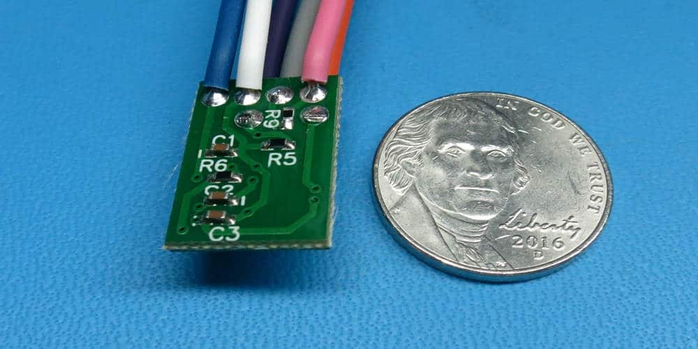
When tech devices either drastically improve their functionality or shrink in size, the electronics industry will collapse. Because of this, Circuit boards can be made much smaller. To help you learn more about designing and fabricating low-volume circuit boards, we’ve included some hints below.
Miniaturization techniques for Printed circuit boards have advanced to the point where a designer can cut their board’s footprint in half or even by a quarter due to the increased complexity and diversity of printed circuit board fabrication. There are the latest design rules which will be required to accommodate smaller vias as well as trace amounts.
Some traditional PCB fabricators may get caught off guard by the move to narrower line widths. Any Printed circuit shop that wants to remain competitive into the foreseeable future. Must provide at least fifty-micron spaces and line segments, preferably no more than thirty microns.
How To Design Micro PCB?
It is obvious that a standard one-ounce copper layer is too thick for use with lines less than thirty microns in width. Thicker lines aren’t sustainable whenever the margin gets decreased. Thinner metal traces shouldn’t cause problems unless you require a lot of current in your layout. To better manage this increased current, a broader, more generalized trace can be used.
Plus, a thirty-micron line is dependable and durable. While a solder mask can greatly improve its durability, it lacks the strength to withstand significant physical abuse.
Many artists may be troubled by these minuscule traces. Nevertheless, they will need to be aware that their initial 200-micron wide trace will eventually narrow to a 25-micron to 13-micron gold or aluminum round wire. Using this wire, the chip carrier can attach to the die.
New techniques for adhering copper towards the surface of a circuit board are helping to improve the micro trace’s overall binding into the board’s ground.
There is a limiting factor in terms of physics for small vias. If the hole is smaller than 2 mm in thickness (or 50 microns), the solution will not plate the wall. Since this happens, the via suffers. The minimum diameter of the via is also determined by the plate thickness.
Everything taken together, the micro via, is really not terrible. Although the micro via is physically smaller than the traces, the microvia’s circumferential ring can be made smaller, allowing for the addition of flavor enhancers.
Space gets saved by using new technology instead of traditional circuit boards for your tiny PCB.
Guidelines For Designing A Micro PCB
Details on how a microcircuit should be laid out have been provided below.

1. Micro vias
High-density interconnect technology involves adding copper layers to the upper edge of a multilayer board or onto a board that is itself a High density interconnect multilayer. To bridge the gap between these incredibly thin layers, micro vias are an excellent choice. The through-holes can be drilled at a depth of 5.9 mils and a radius of 60 mils, or they can be drilled with a beam at a thickness of only 2 to 3 mils.
2. Hole Sizes
To accommodate the micro’s smaller size, every aspect of the Circuit board must be modified from the norm. Expert Circuit design engineers who get used to the standard layout of circuit boards may find this situation difficult. A frequent mistake is to use holes that are too big. Oversized holes in the design can render micro Circuit boards useless or less efficient.
3. Copper Thickness
Standard pattern plating has its uses in microelectronics production. In other words, the trace can remain within the circuit at all times. By plating in a specific pattern, the entire circuit can be more easily connected. Electroless plating, like that used in wire bonding, operates on an electrical rather than a chemical basis.
4. Electrical Testing
The minimum pitch for a rigid as well as the flying probe is between 2 and 3 mils. We anticipate a decline in this as the size of landing strips gets reduced. It has recommended extending the lines away from the circuit if the micro PCBs have smaller points, such as edge strip plugs.
5. Reliability
Normal laminates for PCBs can be used for microcircuits, and high-density interconnects (HDI). But they all have their shortcomings. Micro double-sided and single-sided circuits can be fabricated using strong and stiff FR4 laminates. Micro through-holes, moreover, need to be relatively thin.
6. Security Marking
In order to positively identify printed circuit boards (PCBs), small bar codes can be imaged into the solder mask. Keep in mind that some bar codes are so tiny they can’t be seen by the naked eye.
7. Capabilities of the Supplier
This is a crucial stage in developing any microelectronic-based application but is especially crucial when continuing to work on micro Printed circuit designs.
Keep this advice in mind whenever you set out to do work in Printed circuit board design. The success of your micro Circuit board, however, depends heavily on your familiarity with the company’s offerings and capabilities. For businesses that have never worked on micro Printed circuit designs or collaborated with a Printed circuit fabrication company, this is crucial information.
The reason for this is that each Printed circuit manufacturer has slightly different capabilities when it comes to the manufacturing of microprinted circuit boards. Unfortunately, many Printed circuit manufacturers only offer basic or no micro-electronic support because micro Circuit boards are so novel and complicated. As a result, you should make sure the producer has the resources to fulfill your needs.
Major Applications of Micro PCB
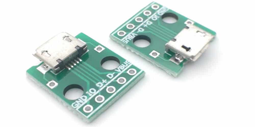
The continuous miniaturization of electronic devices has resulted in or driven the need for denser and smaller PCBs with increased functionality. These days, even the smallest Circuit boards are considered standard. This is due to the increased prevalence of chips with integrated circuits among manufacturers of small Printed circuit designs.
The most compact printed circuit boards (Printed circuit boards) can be used in a variety of contexts and industries.
- High-speed digital/radio-frequency microwave
- Electrical and electronic power supply
- Light emitting diode
- Industrial
- Producing for Others
- Instrumentation
- Besides Semiconductors
Conclusion
Manufacturers increasingly favor miniaturized circuit boards as a result of technological advances. When it comes to miniaturized printed circuit boards, look no further than the Ray Ming Circuit board. Industry norms and customer service are also major topics of discussion. We provide expert services that are flexible enough to meet the fluctuating needs of both low-volume and high-volume production, which runs on small Printed circuit boards. If you need assistance designing a compact Circuit board that will meet your specifications, please get in touch with us right away. Inquire about our flexible pricing options today.
