Electronics are everywhere. From toys to smartphones, all electronics use printed circuit boards (PCBs). The PCB industry has evolved to fulfill the demand for complicated electronic circuits. We’ll only scratch the surface of PCB circuit board creation, which could fill a library.
What Is a Printed Circuit Board?
A stiff causes metal traces and planes to produce electrical circuitry. A circuit board’s electrical circuitry includes components soldered on metal pads. This enables component linking. Boards have many layers, such as one, two, or more circuitry layers.
Circuit boards comprise a low-conducting dielectric material with metal and dielectric layers. This ensures proper conductivity. Circuit lines use copper material such as FR-4 is the common dielectric material for circuit boards.
Board Class
PCBs divides into three distinct classes such as 1, 2, and 3. The PCB’s reliability and design quality indicate its class.
- Consumer electronics come into the category of Class 1 boards.
- Boards of class 2 come in devices where it is desirable but not critical to have a high level of reliability. The goal of these gadgets is to reduce the likelihood of malfunction.
- When it comes to PCBs, the highest quality represents Class 3 boards. If a Class 3 board, such as those seen on airplanes, malfunctions, human lives are in danger.
Different Types of Printed Circuit Boards
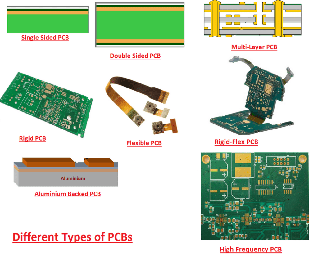
There are three main types Rigid, flex, and metal-core boards.
Many of the boards a designer work with are rigid boards. The board’s layout hides inside a stiff substrate. It is made considering different factors such as a high-heat, high-pressure lamination. Although FR-4 is often used, the material can alter to improve specific features.
Flexible boards bend more than regular boards. It feels like a film roll and is thinner than the rigid board. Flexible boards may enable wearable electronics by removing rigid board devices’ planar restrictions.
Metal-core PCBs replaced stiff boards to keep heat away from critical circuits. This approach may help high-current electronics avoid thermal failure.
Any electromagnetic field-regulated system relies on printed circuit boards. Circuit boards don’t just appear—they require a lot of technical work.
The Process of PCB Design
It is necessary to design a printed circuit board before its construction. The computer-aided design (CAD) software for printed circuit boards makes it achievable. Schematic capture diagrams of circuitry connectivity. The PCB layout builds the physical circuit board. These two are the main PCB design considerations.
Developing the Parts of Library CAD
First, create CAD library parts. Schematic symbols, simulation models, PCB layout footprints, and display schematics are the parts. After finishing the libraries, build a logical circuit diagram. CAD tools connect schematic sheet symbols.
Simulating the circuit ensures the design’s electrical components work. After these processes, schematic tools will give layout tools connectivity information.
Layout Design
In PCB layout, nets connect two or more component pins. Designers use an on-screen sketch of the final board to arrange component footprints. After optimizing these portions, draw the pin traces and planes. CAD tools’ design rules will govern widths and spaces. One net’s traces cannot cross another net’s traces. After routing, the design tools generate manufacturing drawings and output files.
Designing and building a circuit board involves schematic design and simulation, PCB design grid and DRC setup, component placement, PCB routing, power planes, BOM assembly, and board fabrication. The design will prioritize these procedures.

How To Design A Printed Circuit Board?
Even while the design and production of a PCB may be broken down into the broad categories of Printed circuit board assembly, fabrication and layout, the nitty-gritty of each process is quite complex. Some of the finer points of each of these procedures will be examined in this section.
1. Schematic Creation
Starting board design in CAD tools requires completing library part designs. Designing a product requires logic symbols for the resistors, capacitors, inductors, and connectors.
These components are first arranged on schematic sheets using CAD software. After the components are roughly placed, wires can link schematic symbol terminals. Each memory or data circuit has one or more “nets” that connect nodes. Schematic capture requires process component repositioning for clarity.
2. Circuit Simulation
After laying down the circuit’s components and connections, testing is done. The confirmation makes with the use of SPICE, a circuit simulation program. Engineers can test their circuits with these types of tools before physical hardware. These tools are crucial to the PCB design process because of the time and money they can save.
3. CAD Tool Setup
Each design tool has its unique features and capabilities for PCB designers. Design guidelines that avoid net overlap and provide component spacing. Designing grids are one of several techniques designers use to arrange components and route traces.
4. Layout Design Components
The circuit board layout follows the design database and schematic net connectivity data. First, arrange the component footprints on the CAD board according to their outline. When the designer clicks on footprint, a “ghost-line” visual showing net connections appears. Experienced designers will consider connectivity, hot spots, electrical noise, and physical impediments. For example, cables, connectors, and mounting hardware arrange these components for optimal performance. Beyond circuit requirements, design restrictions include how the maker will incorporate components.
5. Route the PCB
Now that everything is in its designated spot (although it can be rearranged if necessary), it’s time to hook up the nets. To do this, the links in the rubber-band net are transformed into lines and planes on paper. It’s possible because of the plethora of tools available in CAD programs, including automated routing functions that cut down on design time significantly. Extreme caution must be exercised during routing to ensure that nets are of the appropriate length for the signals they are carrying and that they do not have noisy pass-through regions. As a result, the manufactured board may experience performance degradation due to crosstalk or other signal integrity issues.
6. Make a Clear Printed Wiring Board Return Path
Integrated circuits (IC) and another active component on the board will often require a connection to a power and ground net. Creating solid planes that these parts can access is as simple as flooding an area or layer. However, it’s not as easy as it looks to build power and ground planes. These wings are also responsible for the crucial task of returning the signals that have been sent along a trace. Besides, it is possible for these return pathways to generate a great deal of noise and reduce the performance of the PCB if the planes have an excessive number of holes, cut-outs, or splits.
7. Final Check
Your PCB design will be complete once you have completed component placement, trace routing, and power and ground planes. Then design the various text and markers that will be silk screened on the outer layers, as well as conduct a final rules check. Marking the board with factors such as names, dates, and copyright information will aid others in locating components. Simultaneously, manufacturing drawings must be produced for use in printed circuit assembly and fabrication. The tools used by PCB designers also help them calculate how much it will cost to manufacture the board.
Design the Circuit Board
The next step is to have the output data files sent to a fabrication facility, as the board is now ready to be produced. Compressing the various metal layers together after being etched with traces and planes produces a bare board suitable for assembly.
A variety of soldering procedures are performed on the board at the assembly site to attach the various components. The completed board then undergoes quality assurance testing before being packaged and sent out for shipment.
8 Golden Rules of printed circuit board design
Despite the increasing availability of powerful and out-of-the-box development boards and system-on-chips for an increasing number of applications, many use cases in electronic devices still require a higher level of semiconductor integration.
However, a custom PCB is still required for use in this application. When it comes to one-time development, even a simple PCB might play a crucial role. In the creation of new electronic systems, the printed circuit board (PCB) is the most adaptable component and the physical foundation for design.
There are different rules such as,
1. Correct Grid Set
Although the multi-grid appears to be functional, engineers can avoid the interval setting. Also, they can maximize the circuit board’s applications by designing a special circuit. Engineers should choose the product that best suits them, such as Polygon is essential for PCB copper. Polygonal copper on multi-grid circuit boards usually fills this geometry. It’s rarer than single-grid designs, yet it can endure longer than circuit boards.
2. Quickest and Direct route
This may seem like a no-brainer, but it should be considered at every step, right down to redesigning the circuit board to shorten the wires.
3. Use of power layer
Most PCB layout programs favor the power layer copper because it is quicker and easier to work with. The most efficient current with the least amount of resistance or voltage drop can be supplied with enough ground return pathways ensured by connecting a large number of wires in parallel.
4. PCB imposition
Picking a size that works well with the maker’s machinery is one way to cut down on the price of prototypes and mass production. Before trying to duplicate your design several times within these panel sizes, you should carry out the circuit board layout on the panel, then contact the circuit board manufacturer to get their recommended size criteria for each panel.
5. Integrating Values of Component
To achieve the same result, a designer may opt for a discrete component with a greater or lower component value. The bill of materials can be simplified, and expenses decreased by integrating into a smaller standard value range. Making the right inventory management decision over the long term is easier if you have a series of PCB goods based on the value of the selected component.
6. Design rule checking
The DRC function in PCB software may only take a few seconds to execute, but it can save a lot of time in the long run if you regularly review your work as you go, especially in a more complex design environment. Maintaining this practice is highly recommendable.
7. The adaptability of Screen printings
Screen printing helps different professionals, such as circuit board manufacturers, installers, and equipment debuggers, with vital label information. Comments can indicate component and connector alignment in addition to marking the circuit board’s functionality and test points. Screen printing reduces manual labor and speeds up assembly.
8. Manufacturing parameters for PCBs
To minimize confusion, produce the Gerber file yourself and use a free viewer to verify it. Most circuit board makers will download and verify it for you. Personal verification do different things such as reveal irresponsible errors, preventing losses from incorrect manufacturing parameters.
Top Printed Circuit Design Programs
1. Eagle
The design named Eagle was developed by German CadSoft Computer GmbH, created by Rudolf Hofer and Klaus-Peter Schmidiger. The company has also been taken over by different brands. These include Farnell and Autodesk. It is a flexible editor for PCB designing and prototypes.
Features
There are many amazing specifications and features, such as:
- Diagram editor, which is useful in different things such as a library, electric rules, and generation of an interconnection list that makes all the processes easier.
- Allows seamless annotation of changes between the diagram and the PCB.
- Diagram hierarchy which renders a better understanding.
- Offers Layout diagrams with advanced features.
2. Altium
The former name of Altium was Protel Systems. The company is based in Australia. It is a supreme software for designing and compiling different PCB models for clients and other companies. The company also boasts a huge consumer base with 5000-6000 users each year.
Features
There are many amazing specifications and features, such as:
- Allows different features such as a Design environment with diagrams, layout routing, documentation, and simulation for attractive PCB designs.
- Design for Manufacturing (DFM) which ensures that your PCB designs are functional, reliable, and easy to produce.
- Allows different data conversion tools for Easy data migration.
- Offers 3D flex-rigid design.
- Enables easy Printed circuit designs.
- It can also work for Diagram designs.
- Allows Production file output also.
3. Proteus
CAD is from Proteus electronics and was developed by Labcenter Electronics Ltd. The CEO of this company is John Jameson. The company operates from the UK. It also has marketing contacts in 50 countries and more.
Features
There are many outstanding specifications, such as:
- The software allows two main software programs, which are helpful in many ways.
- Proteus ISI: It offers diagram creation and electric simulation in an easy manner.
- Proteus ARES: IT allows printed circuit routing solutions with automatic component positioning, which is a quick process due to its functioning.
4. DesignSpark
DesignSpark predicates an electronic CAD software program that has been developed by the teamwork of RS Components and the Number One Systems software developer.
Features
There are many amazing specifications, such as:
- Offers Diagram entry without any technical complications.
- Routing and automatic component positioning are easier with this tool.
- Project interface to organize design files that do not confuse the user.
- 3D viewer, which renders a single view from different angles.
- Lastly, Gerber and Excellon drilling file generation to make things further easier.
5. Protel

As said earlier, Protel is the old version of Altium. The attributes and functions of Protel are variable. It means these depend on the needs and ambitions of different users.
- The latest version is too expensive that is inaccessible to many users.
- Not enough new features to justify the upgrade, which does not make it up-to-date PCB software.
- Not user-friendly and not easy enough to use
- Hardships faced by some users, such as using the new graphic interface.
- Finally, Design-Rule-Check to eliminate any flaws and technical errors.
6. PADS PCB
PADS is developed by CADLOG, which is an effective PCB software for quick and efficient usage and PCB designing. The company is based in Italy. There are many attributes of this too to like.
Features
There are many amazing specifications and features, such as:
- Easy and flawless Diagram entry.
- Component libraries include ParQuest integration and Digikey integration.
- Project rules for easy determination of different functions on the software.
- PCB topology, which offers powerful, interactive routing, DFM and DFT checks, and RF modules.
- Archive management is again a compelling feature of the tool.
Frequently Asked Questions
How to design a printed circuit board?
A PCB is a special type of circuit board that contains all the components on metallic surfaces, namely traces. The circuit board components are on the PCB with a solder mask in the layer of metal pads. It keeps the components intact and also in one place.
Is AutoCAD useful for PCB design?
AutoCAD PCB designer is among the most worthy tools in this pursuit. It also helps with the domains such as electrical or mechanical engineering. However, in some cases, these tools are limited to functional requirements for making tech-based and highly advanced gadgets and electronic components. This is why it is better to use ECAD tools instead of using AutoCAD PCB layout software.
Which material is best for PCB?
Printed circuit boards (PCBs) are flat to appear. The manufacturing material is a kind of composite obtainable from different materials, such as non-conductive substrate materials. Manufacturers pack these with different things such as copper layering, which stabilizes the interconnections of electricity on all counts.
Final Verdict

PCB might be dysfunctional due to technical flaws such as leakage resistances, IR voltage drops in trace foils, Vias, and ground planes, and the influence of stray capacitance and dielectric absorption (DA). PCBs are most likely to absorb moisture due to climatic changes.
Grounding is a broad concept that comes under this discussion. It is the issue that gives rise to analog and mixed-signal designs. There are exceptional attributes of PCB, which are thermal stability, resistance to oxidation, acids, bases, and other chemical agents like alkalis.
Experiments are being on to inculcate additional features such as excellent dielectric properties, water insolubility, the ability of soldering, reliability, and reduced risk of moisture intrusion.
