To make a wise choice when purchasing a multilayer ceramic Printed circuit board, you must understand various factors. This includes features, layer thickness, fabrication process, material quality, performance criteria, and uses. Considering these aspects, you can select an appropriate ceramic printed circuit board for your needs.
What is Multilayer Ceramic PCB?
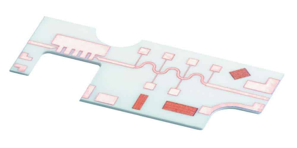
Ceramic PCB is a printed circuit board. It uses a ceramic base material, such as alumina, aluminum nitride, or beryllium oxide, to conduct heat. These materials have a thermal conductivity of 9-20W/m. They allow them to transfer heat away from hot spots and dissipate it over the entire surface. Ceramic PCBs are a mixture of ceramic powder and an organic binder. They are designed in such a way that they are thermally conductive and are made using LAM technology. LAM (laser rapid activation metallization) allows simpler and more efficient construction. Ceramic PCBs offer versatility and improved performance.
Benefits of the Multilayer Ceramic PCB
Ceramic multilayer PCBs (printed circuit boards) has several benefits compared to regular PCBs.
- Ceramic PCBs with multiple layers is excellent at conducting heat. They also have a low thermal expansion coefficient.
- Due to this, they are suitable for use in circuits requiring high power and stable performance.
- The multilayer ceramic Printed circuit board has a simple design and performs well.
- So you can use it as an alternative to long-established traditional circuit boards made of ceramic.
- The multilayer ceramic PCB has many practical uses. It performs well in various situations. It is a versatile and reliable component.
- PCB is beneficial for circuits with high power requirements. It is also used for mounting chips on the board’s surface as modules.
- Furthermore, they can operate at high temperatures exceeding 300 °C. As a result, the board withstands external temperature changes without impacting its performance.
- Although Multilayer ceramic Printed Circuit boards are fabricated to be smaller, their functional reliability is admirable. Thus, appliances that incorporate these small circuit boards can be more compact and portable. They have impressive frequency performance and fewer interfering signals during transmission. This is facilitated by exclusive signal planes.
- They are generally more cost-effective than boards with a single layer. It is possible to fit a more significant number of layers in a smaller space using a multilayer design.
- Moreover, you can enclose multilayer ceramic PCBs in airtight casings. This prevents moisture infiltration. So, the dielectric properties of the printed circuit board will not be compromised.
Uses of the Multilayer Ceramic PCB

Considering the additional board space and circuitry on the multilayer PCB, it has several uses.
- Multilayer ceramic PCBs are used for memory modules. The agglomeration of integrated circuits can produce these modules in a four-layer structure. This device offers a high density and great performance, thanks to its multilayer ceramic PCBs.
- Their use in space developments like satellite communications systems and space vehicles will be amazing. Ceramic multilayer printed circuit boards are preferred for these types of applications. This is due to their ability to perform under difficult conditions. The endurance of multilayer PCBs to shocks, vibrations, and high temperatures is impressive.
- In electronic gadgets, multilayered ceramic PCBs are used. Multilayer configurations are useful for attaching a higher number of electronics. As a result of this implementation, the performance of the gadget is enhanced.
- It is also used in transceiver modules as an additional application. Specifically for radio detection and ranging communication, a multilayer ceramic PCB is used. RF signals are transmitted and received by the module. As the heat conduction capability of aluminum nitride is more compared to alumina, it is used for the ceramic base here. In addition, it offers an optimal communication path with a low CTE.
- Multilayer ceramic printed circuit boards are used to develop analog and digital circuits. So, parasitic traits have manifested less capacitance. Furthermore, the PCBs’ weight and size have been significantly reduced. Interference signals like crosstalk have been reduced and, in some cases, eliminated.
Packaging of Multilayer Ceramic PCBs
The packaging of multilayered ceramic Printed Circuit boards serves two primary purposes.
- Optimizing thermal performance
- Ensuring reliability through hermeticity
The thermal performance can be improved by attaching the PCB to a copper heat sink. We can verify the reliability through hermeticity testing at various extreme temperatures.
Substrates of Multilayer Ceramic PCBs
To transfer electrical charge, substrates provide an electrical barrier between layers. This is especially important in multilayer configurations to prevent signal interference.
The ceramics substrates are made from delicate compounds like alumina or aluminum nitride. They have superior thermal properties when compared to other substrates. Other ceramics, like beryllium oxide, can be used as substrates, but its toxicity limits its use.
Furthermore, we can mold alumina into various strains through injection molding. Zirconia-reinforced aluminum oxide compounds are one example.
