HDI multilayer PCB has gradually become a quantum leap in our world today. For the past few years, HDI multilayer boards have been influencing the whole technical field. These multilayer boards are different from standard multilayer boards. Also, HDI multilayer boards integrate more interconnections than standard PCBs.
HDI called high density interconnect, is a board with pin density within the range of 120-160 pins for each square inch. This board is available in different layers. This article majorly focuses on HDI multilayer boards.
What is HDI Multilayer PCB?
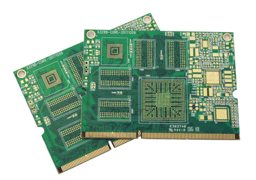
HDI multilayer PCB is a multilayer circuit board that features several interconnections. In this board, the elements are closely positioned to each other to provide a compact look to the printed circuit board. Distinct technological fields like automotive and military utilize this board. An HDI multilayer PCB enhances signal integrity and changes the overall performance of the board.
HDI circuit boards were specially designed to provide an enhanced level of performance and computational power in a smaller space. The demand for more powerful and smaller devices from industries like telecommunication pushed the development of this board. However, there were other major factors that contributed to the development of HDI PCBs. One of these factors is the trends in IC technology.
These trends made PCB manufacturers reconsider the design of PCB interconnects and layouts. Also, HDI multilayer PCB has the ability to package more power in a smaller footprint. This ability of this board to do this lies in the integration of new interconnect techniques like vias in pad and micro vias.
Benefits of HDI Multilayer PCB
HDI multilayer PCB offers several benefits when used in applications.
Highly reliable
Unlike a standard multilayer board, an HDI multilayer is very reliable. The integration of piled vias in this PCB provides maximum resistance power and strength to the PCBs. Therefore, you don’t have to worry about the performance of this board once you invest in it.
Reduces additional charges
When you invest in this board, you will get great value. An HDI multilayer board guarantees ample performance and quality without any extra charges. This PCB serves as an all-in-one PCB. Therefore, you don’t need several standard circuit boards for several applications once you have an HDI board.
Enhanced electrical performance
HDI PCBs have more transistors and a shorter distance between components. This can help to improve electrical performance. Also, these features enable low consumption of power, which enhances signal integrity in the long run.
Lower weight and smaller size
You will be able to secure additional components on both sides of this board. Also, this board enables more functionality while minimizing its weight and size.
Design Considerations for HDI Multilayer PCBs
The production processes of an HDI multilayer PCB are different from those of multilayer standard PCB. Also, the production of HDI multilayer boards begins with the design. The design process of an HDI multilayer PCB is very complex due to the need to consider some physical, thermal, and electromagnetic factors. There are some design considerations to put in mind during the production process.
Via fill types
The specific application and PCB requirements will determine the via fill types. The types of via fill you use should always match the application of the PCB. Also, there are several types of via fill such as conductive epoxy, electrochemical plating, and non conductive epoxy among others. The non conductive epoxy is the commonest via fill type.
Sequential lamination
During lamination, the PCB designer combines PCB cores with copper by applying pressure and heat. Also, the number of layers of a board determine the amount of pressure and heat needed. After the completion of the lamination stage, the PCB designer will have to drill vias. HDI multilayer boards usually undergo the vias drilling several times. Also, sequential lamination prevents breaking and shifting during drilling.
Laser drill technology
Multilayer HDI designs often need laser microvias. These microvias are usually created with laser drills. Also, these drills often generate about 20 microns laser in diameter. This laser can cut through glass and metal and as such, creates very clean tiny holes.
Impedance control
When designing HDI multilayer PCB, designers need to maintain tolerances within +- 10% on trace widths and dielectric layer thicknesses to guarantee that impedance doesn’t affect signal integrity.
Applications of HDI Multilayer PCBs
The HDI technology plays crucial roles in most advanced technologies. Also, electronic components’ miniaturization has helped manufacturers to design smaller devices without compromising reliability and performance. An HDI multilayer PCB is ideal for use in several applications such as:
Communications
HDI multilayer PCBs are widely used in equipment that enable communication devices to function. These boards are available in modules, routers, semiconductors, and switches. Also, digital audio and video equipment often integrate HDI multilayer PCBs. These boards are commonly used in personal communication devices.
Medical devices
HDI PCBs are ideal for use in advanced electronic medical devices like monitoring, imaging, and laboratory analysis equipment. These boards improve the performance of devices when integrated in them. Also, HDI multilayer boards improve the accuracy of medical testing and monitoring.
Automotive and aerospace
With HDI boards, electronic manufacturers can fit more capabilities in very small spaces and devices. In the aerospace and automotive industries, lower weight and smaller space matters. Therefore, HDI multilayer boards are highly preferred to standard multilayer boards in these industries. Modern cars are more computerized and connected.
There are several microprocessors in today’s cars. These microprocessors are crucial in safety, control, and diagnostic features. Also, many features like rearview cameras, GPS and WiFi depend on HDI multilayer PCB.
Industrial uses
Today’s industrial equipment is more computerized than ever. Also, IoT devices are widely integrated in warehousing, manufacturing, and more industrial settings. Most advanced industrial equipment integrate HDI technology. Also, businesses nowadays integrate electronic tools to keep record of inventory and as well monitor equipment performance. Furthermore, machineries are now integrating smart sensors to collect usage data.
Conclusion
An HDI multilayer PCB serves as a crucial driver for the development of several modern electronic devices. With the development of more compact and miniaturized electronic devices, there is more likelihood to integrate HDI technology
