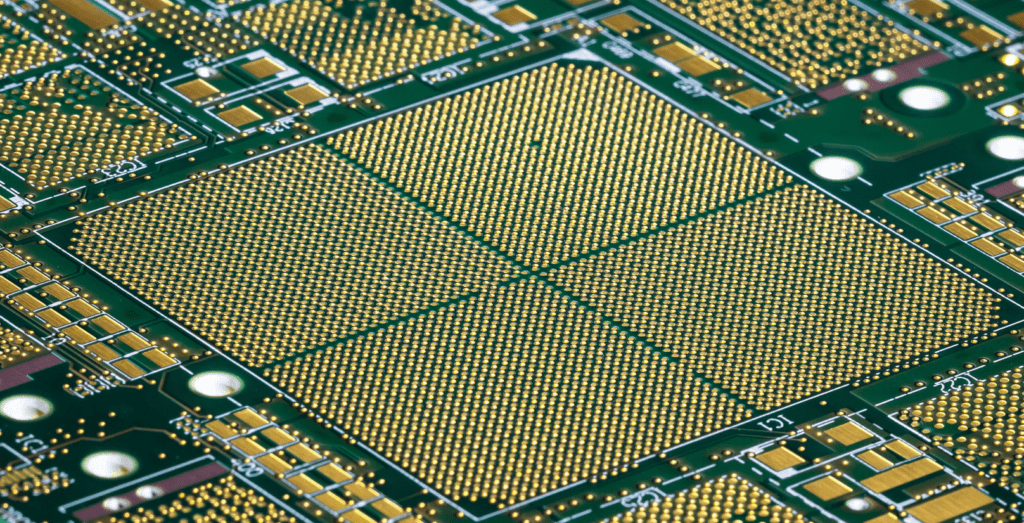
HDI printed circuit boards are becoming a very significant part of electronics industries and PCB. In addition, electronic components have now become more lightweight and smaller. However, it still demands an ever-improving performance. Therefore, to be able to accommodate this, there is a need to pack additional functionality into the smaller area. This is what the HDI PCBs provide.
Do you wish to have mass or small scale fabrication of the HDI PCB? This is the guide that you have been searching for. This article will cover the main aspects of HDI boards, these include the benefits, applications, etc. When you are done reading this article, you will surely become an expert in HDI PCBs. Let’s continue.
What is a HDI PCB?
Compared to the conventional PCBs, the HDI PCBs feature a higher circuitry density. Furthermore, they utilize a combination of blind and buried vias, coupled with microvias, having a diameter of about 0.006” or less. Furthermore, the HDI printed circuit boards are circuit boards having the features below.
- Buried vias and through vias
- Minimum of two layers having through vias
- Through vias from one surface to another surface
- Passive substrate constructions, which feature no electrical connections
- Coreless construction with some layer pairs
- Other constructions of the coreless builds having layer pairs
Furthermore, HDI technology in the printed circuit boards sector as well as other areas has been a major driver for the development of many electronics in use today. These include those which have experienced a substantial decrease in weight and size recently. The smaller this equipment gets, then the more likely it will employ the HDI technology.
This tight technology, which is useful when working with the HDI printed circuit boards, indicates that you have to collaborate with a partner that is experienced. When you have a little layout mishap or small defect, this could cause huge problems.
As one of the leading suppliers of HDI PCB, we have what it takes to provide you with high-quality boards, featuring a greater circuitry density compared to the traditional PCB.
What are the Benefits of Making Use of the HDI Technology?

The HDI technology offers different benefits over all other options, which has the ability to improve your project’s results. Working with the right supplier and right design, making use of HDI boards in your products could improve its overall performance and quality, coupled with high rate of customer satisfaction.
Below are some other benefits of making use of the HDI Technology.
Lower weight and smaller size
When using HDI boards, you will be able to secure more components on the two sides of your bare PCB. This allows you to have better functionality from a smaller space, as well as expands the equipment’s capabilities. In addition, with HDI technology, you will be able to add more functionality and reduce the products’ weight and size.
Improved Electrical Performance
When there is a much shorter distance formed between the components coupled with more transistors in place, this could indicate an improved electrical performance. With these features, you’ll achieve a lower consumption of power. This helps in improving signal integrity. In addition, smaller sizes lead to faster signal transmissions, as well as higher reductions in the overall crossing delays and signal losses.
Increase in cost-effectiveness
When there is proper HDI PCB manufacturing and planning, some HDI boards could become more cost effective compared to other options. This is because they only need less raw materials as a result of the few layers and smaller size they require. For products, which would have initially needed many traditional printed circuit boards, you may just make use of a HDI board. In addition, you’ll get additional value and functionality out of a less material and smaller area.
Enhanced Reliability
Smaller aspect ratios, as well as high quality construction of the microvias has the ability to increase your board’s reliability and that of your product overall. Furthermore, the improved reliability and performance of HDI PCBs leads to customers that are more satisfied and reduced costs.
Quick Production Times
Having the ability to make use of fewer materials, as well as fewer boards, in combination with the design effectiveness that are linked to the high density interconnect technology has the ability to translate into quick production times, as well as a shorter timeframe that is required to get your products into the market.
In addition, placing components into the HDI PCBs are easy to achieve. Also, with a high electrical performance, you will be able to reduce the required time for troubleshooting and testing.
What are the Design Considerations for the HDI PCBs?
All the processes that are involved in producing the HDI PCB are usually different compared to those used with other types of PCBs. Below are the things you need to know regarding the HDI board production as well as some design considerations you will wish to take note of all through the process of production.
Via in Pad Process
The process of via in pad production allows users to place the vias in the flat lands surface on the PCB. You achieve this through the plating of the via, and then filling it using one of the different fill types, then capping it and eventually plating over it. In addition, the via in pad process takes place in about ten to twelve steps requiring skilled technicians and specialized equipment.
In addition, the via in pad is a great choice for the HDI PCB. This is due to its ability to simplify the thermal management, produce very quick ways of bypassing capacitors for the high frequency designs as well as reduce the space requirements.
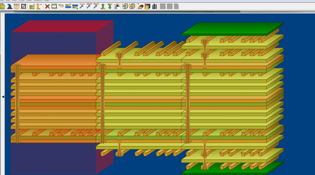
Sequential Lamination
During the lamination process, the printed circuit board cores are combined making use of copper coupled with prepreg layers for the multilayer pcb through the application of pressure and heat. After completing the lamination phase, the PCB manufacturer then drills vias. In contrast to other printed circuit boards, the HDI printed circuit boards pass through the whole process many times.
Types of Via Fill
The types of vial fill have to match the requirements of the printed circuit board and the application in question. In addition, the via fill materials include non-conductive epoxy, conductive epoxy, copper filled, silver filled, electrochemical plating, etc.
Laser drill technology
High density interconnect design needs laser microvias that are created using the laser drills. The drills usually generate laser direct imaging with a diameter of 20 microns. This helps in cutting through glass and metal effortlessly, and also creating tiny and clean holes.
What are the Applications of the HDI PCB?
High density interconnect technology is a very important component found in many advanced technologies of today. Below are some of the industries making use of the HDI PCB and ways of using them.
Consumer Electronics
Back then, computers used to occupy a whole room. However, thanks to the high density interconnect technology, devices that are as small as smartwatches are just like personal computers. HDI printed circuit boards are seen in wearables, tablets, smartphones, and laptops and consumer electronics such as GPS devices and digital cameras.
Aerospace and Automotive
The HDI PCB permits manufacturers to be able to fit better capabilities in smaller devices and spaces, which weighs less. This feature is very important in the aerospace and automotive industries, whereby lower weight could mean better operation. Majority of new features like onboard GPS and WiFi, backup sensors and rear view cameras rely on the HDI PCB.
Communications
Asides laptops and smartphones, the HDI PCB appears in the equipment, which permits the functioning of these devices like semiconductors, modules, switches, and routers. When making use of electronic communications, there is a chance you are making use of HDI printed circuit boards.
Industrial Uses
As of today, industrial equipment are now becoming computerized. This also holds for IoT devices that are now more common in warehousing, manufacturing, as well as other industrial settings. A good number of these advanced equipment uses the high density interconnect printed circuit board technology. Also, businesses make use of electronic tools in keeping track of the inventory, as well as monitor the performance of the equipment. This is why HDI printed circuit boards are important.
Medical Devices
The advanced medical devices, which include some equipment for laboratory analysis, surgical procedures, imaging, and monitoring, may incorporate high density interconnect PCBs or the HDI PCB. In addition, the high density interconnect PCB technology helps in promoting better performance. The HDI printed circuit board also improves the accuracy of medical testing and monitoring.
What are the Cost Considerations of High Density Interconnect PCBs?
There are some factors that affect the cost of HDI density interconnect PCBs.
- Number of layer and the stackup height
- The materials you are using
- Staggered vs stacked
- The sequential laminations
- Amount and type of microvias, through-holes, or vias
- The HDI printed circuit board supplier
- Turnaround time
- Size of the pad
Conclusion
HDI technology enables electronic components to become more lightweight and smaller. Furthermore, you can incorporate HDI boards into different applications.
