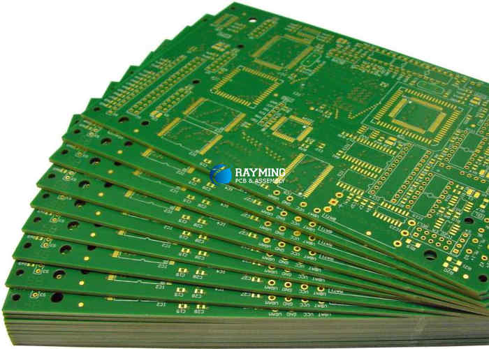
Electronic circuit boards come in diverse types, sizes, and levels of sophistication. However, the printed circuit board represents arguably the most popular in diverse sectors of the global economy. Almost all electronic devices rely on PCBs to function. Its manufacturer, therefore, becomes of central interest to any circuit board enthusiast. The quality of PCB products correlates to the capability and pedigree of the PCB manufacturer. Therefore, understanding the manufacturing process, types of services, and how to pick a top PCB provider becomes necessary for your business.
Services Offered by PCB Manufacturers
The manufacturing of printed circuit boards entails an end-to-end process involving design, prototyping, fabrication services, assembly, and packaging. Different people will have distinct PCB needs based on their capability and budget. It is not strange to find customers who can design their PCBs but rely on PCB makers for fabrication or assembly needs. It can include their PCB prototype or low-volume production but, at times, mass or high-volume production. Some clients, however, only engage PCB manufacturers for their printed circuit board assembly needs. Others shift all their PCB needs to their electronic contract manufacturer.
An In-depth Look at the PCB Services offered by Manufacturers
Design of Printed Circuit Boards
It often represents the first and the most fundamental step of the production or manufacturing process of PCBs. Most PCB enthusiasts and engineers design their PCBs, though PCB manufacturers offer valuable input in such design processes, including corrections. In some cases, a PCB manufacturer will provide the entire design process.
The insights you will get from PCB manufacturers regarding the design can include aspects ranging from the steps, design considerations, applicable PCB design software to use, etc. the following represents the highlights of the design insights you might receive from PCB manufacturers.
- It entails comprehending the electrical considerations, developing the schematic, deploying the schematic capture tool to develop the PCB layout, and designing the printed circuit stack-up. After that, defining the design rules and needs, placing components, routing traces, incorporating identifiers, and generating the layout or design files ensue.
- Design considerations. Critical insights on the design of PCBs include the size of traces, ensuring the smaller loops, proper placement of the decoupling capacitor, Kelvin connections, and keeping the noisy and digital traces apart. Other critical aspects to consider including the number and size of vias, heatsink positioning, thermal vias, and the spacing of mounting holes to traces. Considering heat-sensitive components also becomes necessary.
- Printed circuit board design software suites
- Plenty of PCB design software exists. Most of the design suites can have a limited amount of output file formats. A key insight from PCB manufacturers entails using an open-access software that can design and output the layout file in an acceptable format – mostly Gerber file format. Some of the design software suites include KiCAD, EAGLE, PCB Designer, etc. All of these PCB design suites have their benefits and drawbacks.
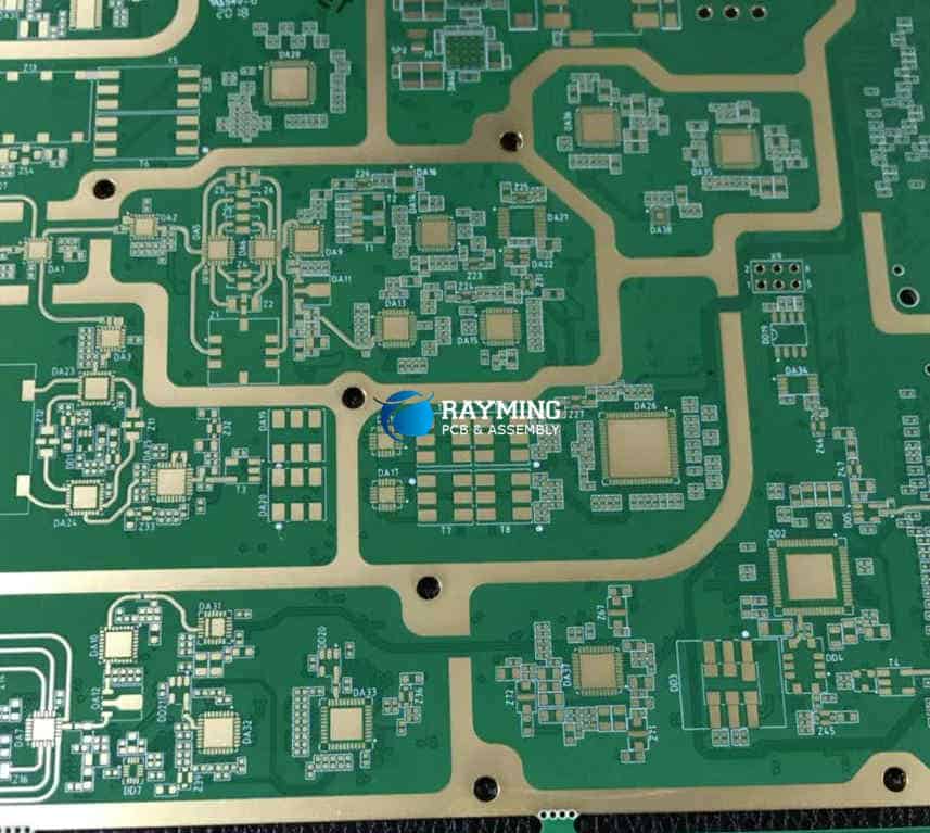
Fabrication of Printed Circuit Boards
Fabrication of the bare boards is a vital service that most PCB manufacturers provide. The fabrication process can happen at the prototype level or high-volume level. Bare boards become essential in the manufacturing and assembly process, which turns them into printed circuit boards. A bare board consists of the non-conductive substrate material sandwiched between the conductive layers of copper. However, the copper layer or layers depending on the type of bare PCB needed.
PCB fabrication covers every type of PCB, though some PCB manufacturers have limited fabrication capability. RayMing PCB and Assembly is an excellent PCB manufacturer that can satisfy your fabrication needs of diverse PCB types. What’s more? It includes single-layered, double-layer PCBs, multilayer PCB. Printed circuit boards also come classified based on the type of material and design software used. As a result, you will also find PCBs such as Arlon PCBs, EAGLE PCBs, metal core pcb etc.
The basic fabrication requirements for PCBs entail a design checklist. It includes the following.
Circuit Board Particulars
Aspects captured here include the circuit board configuration and stack-up, minimum trace spacing and width, controlled impedance layer, and copper balancing. It also entails Via structures and types besides copper balancing.
Finished PCB Design
It is prudent to ensure the PCB design proves complete to ensure accuracy in the PCB’s manufacturing process. When not adequately synchronized with the layout and schematic, a simple part or component update can result in a bad circuit board. The checklist, therefore, encompasses the following before it enters fabrication.
- A synchronized and updated layout ad schematic database
- Ensuring the circuitry passes through a comprehensive engineering review
- All components or parts get placed appropriately on the circuit board besides ensuring that every net connection proves routed.
- That the BOM gets reviewed for available and current components
- Printed circuit board design constraints and rules get checked and the present errors corrected
- Circuit simulation, power integrity, and signal integrity analysis gets completed
- That DFM or design for manufacturing rules get reviewed to ensure an error-free assembly
A Complete Manufacturing design Data
It applies to post the completion of the PCB design and before the fabrication process starts. It entails the generation of assembly and fabrication data files that get submitted to an electronic contract manufacturer. The files become instrumental in conducting design reviews before forwarding them to get the raw material quote. It includes the following.
- Gerber files or any other formatted mage files of the board layer
- BOM or bill of quantities
- Manufacturing drawings for assembly and fabrication
- Schematic
- Netlist
- Pick and place locations of the components
- Test point spots
A Typical Fabrication Process Handled by a PCB Manufacturer
Printed circuit board manufacturers often start the board’s fabrication process once they receive the necessary design data and information. Well, the down payment of the associated fabrication costs depends on the PCB supplier or manufacturer. But what steps do PCB manufacturers undertake?
Steps
Developing the Circuit’s Image
It is the initial step and entails transferring the printed circuit board’s design image data from the Gerber file into the board. It is, however, prudent to note that as much as the widespread and acceptable format comes as the Gerber, other formats exist.
The image creation can happen in either direct imaging or photo tooling. Photo tooling involves a process where a photo-plotter creates the circuitry photos on films, acting as templates for printing them on the circuit board. On the other hand, direct imaging involves a laser printer that directly prints the board images. Direct imagining bypasses the need for photo tooling.
Developing the Circuit Board Layers
It primarily works for double and multilayer PCBs. Such circuit boards have diverse dielectric layers with metallic traces for conduction. Multilayer boards use thinner versions of the core structure primarily deployed in double-sided circuit boards. It then laminates it with other structures to develop the circuit board’s layer stack-up. Regulation of aspects like copper weight, width, and layer-to-layer alignment becomes essential if you target high quality.
Developing the Circuitry of the Inner Layers
It entails a process of printing the circuitry image into the inner layers of the circuit board. The core’s copper foil gets covered using a photoresist material which then has to get exposed to UV via direct imaging or photo tooling. The regions or spots containing the circuitry hardens the material (photoresist) before removing extra and unhardened photoresist using a chemical solution process. AOI then commences upon completing the inner layer circuitry development before the layers get laminated into a single complete electronic circuit board.
Lamination of the Layers
It involves stacking the layers containing the thin copper sheets covering the top and bottom external surfaces to form a PCB sandwich. Prepreg needs to get applied to each layer to enhance the bonding process. It is a delicate process that needs plenty of attention to ensure a proper circuitry alignment on the diverse layers.
Drilling of the Holes
The step follows the stack-up layer lamination process. Holes have to get drilled into the board to facilitate the mounting of components through the plated through-hole technology. The drilled holes have to get cleaning using a mechanical and chemical process. After that, the surface of the board (both external layers and the hole surfaces) gets coated with copper. It creates a base that can get used for electroplating extra copper.
Creating the Bottom and Top Layer Circuitry
A similar process of printing the circuitry images as already completed for the inner layer gets underway. However, while the photoresist still gets deployed for the outer layers, the circuit has to stay unprotected and plated using the extra copper.
Application of the Solder Mask, the Silkscreen, and Surface Finishes
The board often needs protection during the assembly process. Because of this, solder mask application ensues using an ultraviolet exposure process. It is similar to the photoresist treatment. The solder mask gets applied to the whole surface save for the metal pads needed for soldering. Further, reference designators for components besides other markings get silkscreened onto the circuit board. Silkscreen and solder mask get cured through a process of oven baking. The exposed metal surfaces also receive a surface finish to help protect it besides assisting in the soldering process during assembly.
Assembly Preparation, Inspection, and Testing
It comes as the last step in the fabrication process of PCBs. This stage prepares the printed circuit board for the assembly process. Whenever necessary, the circuit board gets routed or prepared using the V-cut along the board’s outline. After this, the board must pass through a continuity test using automatic testing equipment like the flying probe or bed of nails test fixtures. The aim of the tests entails identifying unintentional shorts. Post the completion of this process; the board becomes ready for the assembly process.
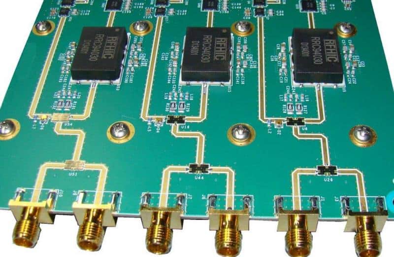
Printed Circuit Board Assembly
Assembly of PCBs encompasses another vital service offered by most PCB makers. It can either involve PCB prototype assembly or mass assembly based on the customer’s needs. The assembly process ensures that all relevant electronic components get placed and soldered into the board’s circuitry. It often involves both passive and active components with different numbers based on the type and complexity of the PCB design. The copper traces on the bare boards electrically connect the components to the connectors.
PCB assembly can happen either through surface-mount technology or plated-through hole technology approaches. The surface-mount tech approach entails mounting the electronic components directly onto the circuit board’s surface. It is one of the popular and preferred methods of assembling SMDs in the industry. SMT enhances manufacturing automation that in turn cuts on costs and boosts quality.
The through-hole technology method uses leads to fix components into the circuit board. The mounting process inserts the component leads into the drilled circuit board holes before soldering and fixing them in place. Soldering can happen through manual soldering or wave soldering. Based on the type of PCB and the targeted application area, either assembly method can apply. However, plated through-hole technology applies mainly to PCBAs that operate in tough environmental conditions experiencing lots of vibrations. However, SMT manufacturing can apply to PCBs targeting different application areas. Remember that both approaches can get utilized simultaneously in the assembly of a PCB.
Assembly Process
Most, if not all, PCBA companies like China PCB have a similar printed circuit board assembly process for different types of PCBs. The process followed often involves the following steps.
Through-Hole Technology Approach
- Component assembly where the parts or component’s leads get inserted through the board’s drilled holes
- Inspection and rectification of errors regarding the component placement
- Wave soldering, where a single side of the board gets exposed to the solder. Components get soldered simultaneously as it passes through this process.
Surface-Mount Approach
- Application of the solder comes as the first step. The solder paste holds the parts or components in readiness for the soldering process.
- Mounting of components then ensues. Here the components get laid or placed on the conductor pad footprint.
- Reflow soldering then gets performed where the board passes a reflow oven with temperatures reaching 235°C.
In most instances, it becomes appropriate to institute aspects such as DFM and DFA for the fabrication and assembly of printed circuit boards. It helps avert some of the potential assembly errors before the onset of the assembly process.
Component and Material Sourcing
It is a service that almost every top PCB manufacturer provides to their clients, especially for PCB’s full turnkey manufacturing and assembly service. The components sourced can involve passive and active components (transistors, capacitors, connectors, etc.) However, it requires that the client or customer submits a detailed list together with their PCB design files.
A PCB manufacturer also sources materials like conducting copper, non-conducting substrate materials, surface finishes, etc., based on the customer’s PCB design needs as specified. For instance, a PCB supplier will source for RF4, Arlon, or Ceramic substrate materials based on the type of PCB and the BOM (bill of materials) submitted.
Sourcing of components and materials can happen in-house or through outsourcing channels. However, either means tends to benefit both the PCB manufacturer or assembler and the customer when it comes to cost and time-to-market periods. It primarily arises from the economies of scale that most PCB manufacturers enjoy. Another key reason for this gets established and excellent supplier relations, which brings discounts on materials or components sourced.
Other Services
PCB manufacturers provide solutions that transcend fabrication, assembly, and materials or component sourcing. A lot of top-tier PCB solutions providers offer customer care services besides delivery services. For instance, prompt responses to questions regarding PCB manufacturing capabilities or other aspects become useful in developing trust and lasting relationships.
The Importance of Choosing a PCB Manufacturer for Your PCB Needs
Picking a suitable PCB manufacturer becomes pivotal in ensuring the quality and timeliness of your printed circuit board products. It also helps find new ways of scaling down expenses, especially for original contract manufacturers. But what is the significance of finding a suitable contract PCB partner for your needs?
Reasons
Enhanced production accuracy and speed
High printed circuit board quality besides minimum time-to-market period act as prerequisites of success in the PCB industry. The presence of advanced facilities and technologies, trusted, experienced, and knowledgeable ECMs guarantee high quality and shortened lead times. What’s more? The ECMs test the boards in the actual environments under the expert watch of professionals.
Limited design time
The PCB design process and its time can act as a source of concern for most electronic component companies. It further worsens the time required to fabricate and assemble PCBs, especially when it is complex. Relying on an ECM overcomes these issues and other difficulties because of their wealth of expertise and experience.
Getting all the required services from the one-stop-shop PCB companies
Most OEMs receive a range of services from their ECM (electronic contract manufacturers). Most highly experienced ECMs provide end-to-end PCB solutions that cater to diverse electronic needs, including ideation to installation. Therefore, it is not necessary to get in touch with different companies when it comes to, say, your assembly needs. ECMs also provide supply chain-related logistics that hinder most OEMs.
Low costs of operation and enhanced production
Small and medium-sized electronic companies can find it difficult to commit to the large capital investment that PCB manufacturing may require. Consequently, partnering with ECMs can go a long way in keeping their expenses low while guaranteeing themselves increased volumes and an enhanced time-to-market period.
Quick sourcing of electronic components
The associated costs of sourcing for PCB components can prove prohibitive for small and medium-sized companies. Therefore, partnering and having the ECM procure the components on their behalf helps. ECMs can quickly and efficiently procure the parts from their elaborate supply chain contacts easily. Further, the ECM also provides inspection and testing of the parts at no cost.
Eliminates expensive rework
The capacity of ECMs in providing comprehensive testing and inspection comes in handy in achieving a flawless PCB. Such automated and manual testing approaches ensure quality and eliminate the need for any potential rework of the PCB.
How to Find a Suitable PCB Manufacturer
The benefits of getting a top PCB manufacturer or rigid flex PCB supplier can determine the profitability of your PCB enterprise. However, plenty of PCB makers exist, and discriminating between them can become difficult. So can you narrow down the options? Certainly, and the following comprises some of the factors to consider
The company’s capability range
Consider the types of PCB services the company provides. A suitable manufacturing partner has to offer a range of product services like fabrication and assembly of rigid-flex, flex, and rigid PCBs. It should also have the capacity to handle single-layered and multilayer circuit boards.
Service capabilities
It is prudent to check if the company offers a project management option. For instance, do they have policies regarding inventory management, shipping, and warehousing? If so, then get into the specifics to determine a suitable fit.
Quality control
A top and ideal PCB manufacturer should offer in-house design, fabrication, and assembly review. The quality control aspect also assists in speeding up the delivery times. Ensure that the electronic contract manufacturer understands how to test for diverse quality aspects. Additionally, the company needs to demonstrate its capacity by having up-to-date technologies and machines. The company staff needs to show the required consistency of producing high-quality products.
Layout review
A PCB manufacturer needs to facilitate a PCB layout review. Nipping errors or problems at the initial stages becomes crucial before the manufacturing process starts. T can become stressful and costly to rework the entire process after the fabrication and assembly process starts.
Flexibility and ability to respond
It is crucial to consider the possibility of any need arising for changing the project’s specification. The ability of the PCB manufacturer to handle any prompt changes to the project specifications marks their capacity to deliver. Therefore, pick a top PCB manufacturer who can respond rapidly and efficiently to your manufacturing needs without a lot of fuss.
Final remarks
The quality and impact of a PCB product in the market can influence your fortunes in the industry as a small and medium-scale OEM. However, to guarantee this, it becomes necessary to understand how to pick a suitable and top-tier PCB manufacturer and comprehend their manufacturing processes. We hope the insights provided have shaped your thought process regarding the entire PCB manufacturing process.
