LoRa PCB antenna design is a critical aspect of the LoRa technology, which is a low-power, long-range wireless communication protocol. The LoRa protocol is becoming increasingly popular in the Internet of Things (IoT) industry due to its ability to transmit data over long distances while consuming minimal energy. However, to achieve optimal performance, it is crucial to design the LoRa PCB antenna correctly.
The design of the LoRa PCB antenna involves several factors, including the antenna’s size, shape, and placement on the PCB. The antenna’s size and shape determine its resonant frequency, which is critical for achieving the desired transmission range. Additionally, the antenna’s placement on the PCB can affect its performance, as the surrounding components can interfere with the antenna’s radiation pattern. Therefore, it is essential to consider these factors when designing a LoRa PCB antenna to ensure optimal performance.
Lora PCB Antenna Design Fundamentals
Antenna Basics
An antenna is a device that converts electrical signals into electromagnetic waves and vice versa. It is an essential component of any wireless communication system. In the case of Lora, the antenna is responsible for transmitting and receiving signals in the 868 MHz or 915 MHz frequency bands.
The performance of an antenna is determined by several factors, including its size, shape, orientation, and the materials used to construct it. The most common types of antennas used in Lora applications are the monopole and dipole antennas.
PCB Antenna Design Considerations
When designing a PCB antenna for Lora, several factors must be taken into consideration to ensure optimal performance. These include:
- Frequency: The antenna must be designed to operate at the desired frequency band, either 868 MHz or 915 MHz.
- Ground plane: The antenna must be placed on a large ground plane to provide a low impedance path for the return current and to prevent radiation from the ground plane.
- Size: The size of the antenna is critical as it affects the antenna’s efficiency and bandwidth. The length of the antenna must be a quarter-wavelength or a multiple of a quarter-wavelength.
- Matching: The antenna must be matched to the impedance of the transmission line to minimize reflection losses. This is typically achieved using a matching network, such as a balun or matching circuit.
- Radiation pattern: The antenna’s radiation pattern must be optimized for the intended application, such as omnidirectional or directional radiation.
In conclusion, designing a PCB antenna for Lora requires careful consideration of several factors, including frequency, ground plane, size, matching, and radiation pattern. By following these guidelines, designers can ensure optimal performance and reliable wireless communication.
Lora PCB Antenna Design Techniques
Monopole Antenna Design
A monopole antenna is a type of antenna that is commonly used in Lora PCB antenna design. It consists of a single wire that is placed above a ground plane. The length of the wire is typically a quarter wavelength long, and the ground plane is used to reflect the signal. The monopole antenna is a simple and effective design that can be used in a wide range of applications. It is also relatively easy to manufacture, which makes it a popular choice for Lora PCB antenna design.
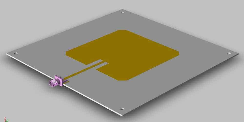
Patch Antenna Design
A patch antenna is another type of antenna that is commonly used in Lora PCB antenna design. It consists of a metal patch that is placed above a ground plane. The patch is typically a quarter wavelength long, and it is designed to resonate at the frequency of the Lora signal. The patch antenna is a highly directional antenna that can be used to transmit and receive signals over long distances. It is also relatively easy to manufacture, which makes it a popular choice for Lora PCB antenna design.
Inverted-F Antenna Design
An inverted-F antenna is a type of antenna that is commonly used in Lora PCB antenna design. It consists of a metal strip that is placed above a ground plane. The strip is typically a quarter wavelength long, and it is designed to resonate at the frequency of the Lora signal. The inverted-F antenna is a compact and efficient design that can be used in a wide range of applications. It is also relatively easy to manufacture, which makes it a popular choice for Lora PCB antenna design.
In conclusion, Lora PCB antenna design techniques are critical in ensuring reliable and efficient communication in Lora networks. Monopole, patch, and inverted-F antennas are the most commonly used designs in Lora PCB antenna design. Each of these designs has its advantages and disadvantages, and the choice of design will depend on the specific requirements of the application.
Advanced Lora PCB Antenna Design

Antenna Matching Techniques
Antenna matching is a crucial part of designing an effective LoRa PCB antenna. The goal of antenna matching is to ensure that the antenna impedance matches the impedance of the transmitter or receiver circuitry. This is important because if the impedance is mismatched, it can lead to poor performance, reduced range, and even damage to the circuitry.
One common technique for antenna matching is using a matching network. This network is typically made up of capacitors and inductors that are placed in series or parallel with the antenna. The values of these components are carefully selected to match the impedance of the antenna to the circuitry.
Another technique is using a balun, which is a device that converts between balanced and unbalanced signals. This can help match the impedance of the antenna to the circuitry, especially in cases where the antenna is unbalanced and the circuitry is balanced.
Antenna Tuning Techniques
Antenna tuning is the process of adjusting the antenna to resonate at the desired frequency. This is important because if the antenna is not tuned correctly, it will not be able to efficiently transmit or receive signals at that frequency.
One technique for antenna tuning is using a network analyzer to measure the impedance of the antenna at different frequencies. The data from the network analyzer can be used to adjust the length of the antenna or the values of the matching network components to achieve the desired resonance.
Another technique is using a frequency counter to measure the resonant frequency of the antenna. This can be done by connecting a signal generator to the antenna and sweeping the frequency until the maximum voltage is reached. The resonant frequency can then be calculated based on the frequency at which the maximum voltage occurred.
Antenna Radiation Pattern Optimization
Antenna radiation pattern optimization is the process of adjusting the antenna to achieve the desired radiation pattern. The radiation pattern is the pattern of electromagnetic energy that is radiated by the antenna.
One technique for radiation pattern optimization is using a computer simulation to model the antenna and predict its radiation pattern. The simulation can be used to adjust the shape and size of the antenna to achieve the desired pattern.
Another technique is using a near-field scanner to measure the radiation pattern of the antenna. This involves placing the antenna in a chamber and scanning it with a probe to measure the electromagnetic field. The data from the scanner can be used to adjust the antenna to achieve the desired pattern.
Overall, advanced LoRa PCB antenna design requires careful attention to antenna matching, tuning, and radiation pattern optimization. By using these techniques, designers can create antennas that are efficient, reliable, and capable of transmitting and receiving signals over long distances.
