Glass is an unusual material that has been around for thousands of years. In the modern era of photonics, glass’s importance as a light waveguide is growing. For greater data transmission. Glass fibers have replaced coiled wire in the last two decades. Information transmission on the circuit board gets taken over by glass. Besides this, the chip level and everywhere in between may soon also get taken over by glass as we transition from electronic data interchange to photonics-enabled data processing systems.
The Fraunhofer IZM is pursuing this line of technology development. Fraunhofer IZM was established twenty-six years ago. Since then, it has accelerated the miniaturization and incorporation of electronic components. It is now exploring the incorporation of photonic technology into ever tinier. And more complicated to manage the exponentially increasing volume and velocity of data.
Optical PCB – From Electrons To Photons
Data analytics, social media platforms, and the IoT are some examples of data processing. They all call for sophisticated data processing architectures. They are currently in development. There is a growing need to figure out how to link together optical processing units as technologies like photonic circuits and light-based supercomputers gain traction.
The use of glass fibers is an excellent alternative for long-distance transmission. However, this method results in a tangled mess of wiring. Not unlike that of electrical appliances from the beginning half of the century. When applied to short ranges, such as inside gadgets. Printable electrical connections are also called pubs. These were developed as a means of reducing the chaos of electric wires (PCBs).
Transitioning from digital to photonic data acquisition isn’t a straight copy-and-paste operation, though. Gadgets for producing, processing, transmitting, as well as getting beams are necessary. Electro-optical conversion, as well as transceiver technology, are some other examples. They provide a high-level overview of the necessary technological building blocks.
The above-mentioned examples represent different technologies that facilitate integration. For example, silicon photonics (green) and improved packaging (yellow) (orange). An upgraded version of the framework for photonic incorporation is predictable for 2019. But it is also notable here that this process is currently underway. Clearly, there is a wide variety of photonic experts that goes far beyond the scope of one article.
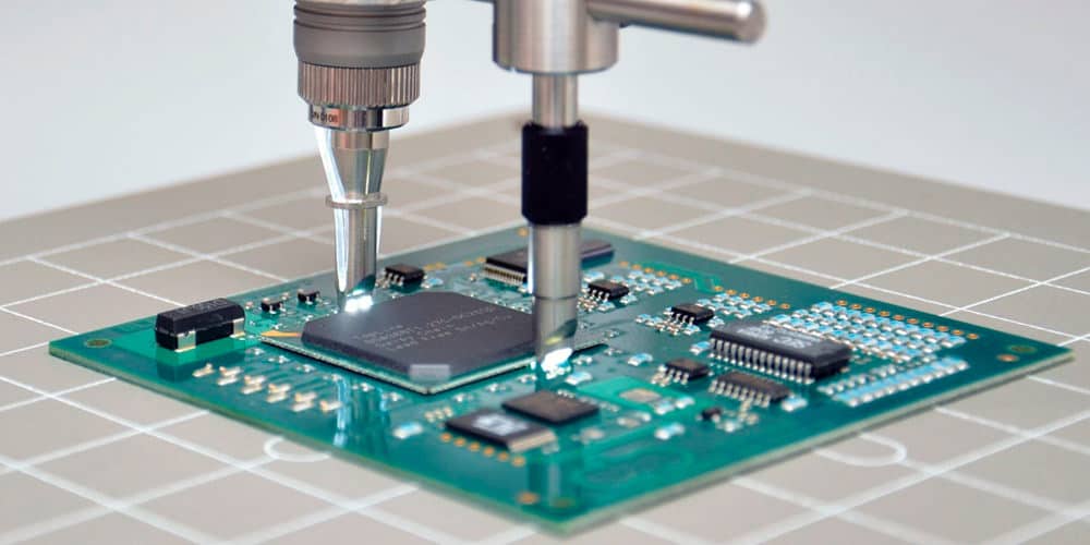
High Bandwidth Optical PCB
The number and size of transistors in IC have both increased over time. Unfortunately, the output in chip production decreases as chip size increases. So, there is a limit to how large chips can get. Consequently, chiplets are used to partition electronic chips into smaller, more manageable chunks. They are available in a variety of places. Some of which can be on interposers. They are a kind of intermediate provider of chipsets. They contain integrated data-transfer structures. Vertical, horizontal, or optical connections are possible with the interposer (or even both).
Physiological limits are being reached as data rates throughout communication systems between electronic processing units continue to rise. High-speed data transmission is also achievable through the use of between chips. Interposers, as well as panels, are also usable. Optical IO units are essential for this method. So, further electro-optic connectivity integration is required. To avoid connection chaos, photonic transmission on PCBs is highly desirable.
Photonics In A Thin Glass

To develop the concept of the electrical circuit board (EOCB). Researchers shifted their focus from the traditional electrical PCB to a photonic solution. The EOCB concept incorporates some ideas from the traditional electrical globe. And use them for the creation of new photonic structures. It gets motivated by the requirement for higher bandwidth. To facilitate data transmission, an EOCB may make use of a layer that conducts light. Moreover, EOCBs must meet a number of general requirements. The lowest possible cost, high reliability, and simple manufacturability. They are among the most crucial.
Thin glass is common in displays. And formalized polymer layers are common in polymer optical fibers. POF are excellent candidates for the light-conducting layer. At telephony wavelengths, a waveguide made of glass is more durable. It can withstand less heat. And it has higher transmission than other materials as cell phone technology has advanced. Thin glass has emerged as a cost-effective, high-quality substitute.
In place of printed steel circuits. Optical fibers can get incorporated by electrostatic interaction. The electrostatic interaction within paper-thin sheets of glass to carry beams. The material and also the technology have demonstrated high long-term consistency. It remains stable even at superior temperature loads. And they are consistent with photonic devices and fiber optics. Producing 305 mm 440 mm EOCBs is possible. Thanks to the well-established processing method for such material.
In addition to traditional electronics, glass’s two unique qualities are as follows due to its high insulating properties. It can get placed in close proximity to live conductors without risk. Glass’s poor thermal conductivity means it is unsuitable for heat transport. This necessitates careful thermal management throughout the design process.
Structure Of Optical PCB
Glass plates could get laminated with regular organic raw products like FR4. The FR4 can create an EOCB. Glass can be utilized as a core layer inside the typically printed circuit base material. Or as the primary carrier material itself. It is a photonic interposer carrying all the PIC and electronic chip components. Glass and organic materials are both palatable with copper. Normal Printed circuit processing can get used, but elevated assembly is necessary.
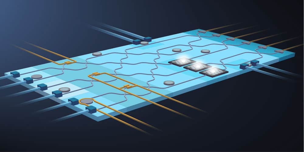
Inside the EOCB, the blue layer signifies a glass substrate. It contains built-in single-mode optical waveguides. The electronic processor sits atop a cooling surface in the form of a glass interposer. Particularly, the interface between both the transmitter and the substrate glass is crucial. There is a well-established method for the construction of TGVs. It allows electrical signals to pass through glass. But directing the photodetector signals is more difficult. There are presently two main methods being developed. One employs a periscope mounted on the upper end of the EOCB. While the other uses a small mirror mounted on the underside. Standardization and multi-source commitments should also be part of the sector. But each of these methods has not yet been developed by the sector.
For this type of EOCB, it is necessary to address a number of design challenges. These consist of electrical properties. These necessitate path optimization as well as signal-reflection removal for RF. Also, they require electromagnetic wave transmission. The optical properties require signal enhancement and free-space collimation. But also optomechanical system design. As well as the thermal properties. They necessitate consideration of heat sources and the integration of the absorber plate. Integrated into a 25 Gbit/s/ch electro-optic transmitter. This photonic interposer is fully functional. TGVs have been manufactured using a galvanic wafer-level process. Light from Vlsi circuits or other lighting effects gets installed on the top of both interposers. It gets collimated by polymer lenses mounted at the endpoints of the lateral optical pathways in the bottle. Which exit the interposer at the bottom. A deflecting mirror component on the internal mechanism can pick up these signals.
Very small optical losses (0.5 dB at the receiver and 2 dB at 2 mm from the polymer microlens) characterize the system demonstrated.
What Is There, & What Is Missing?
In the future, electrical PCBs will be crucial for efficient data processing. Integration of optical connections among electrical and optoelectronics storage and processing units at multiple levels is necessary. Not only from chips and chipsets to interposers but also full panels, is a crucial need. This problem is resolvable using waveguides made through an atom process in inexpensive display windows. The windows get laminated with regular Printed circuit materials. All the steps in the processing chain get refined to work with a full plate thickness of 610 mm and 440 mm. So, the next step is to implement them in mass production. Ideally, using existing printed circuit board production lines. Many difficulties persist. For instance, several approaches have been proposed for improving TGVs’ connector orientation. But no consensus has been reached.
