Using antennas in a PCB can help extend and bolster the signal transmission, as well as aid in cost reductions. The use of the PCB patch antenna has been discovered to also be a factor in the physical footprint reduction too.
In this article, we talk about the meaning of this type of antenna, the benefits and some of the additional pieces of information you need to know.
What is a PCB Patch Antenna?
It is a dedicated, robust planar structured and low-profile, bidirectional radio antenna mainly used for creating a field between the patch’s edges. This is done in a way that the voltage located at one end of the patch is higher than the other, while enabling a differential polarization of the fields from each side of the patch.
This optimization is the reason why the circuit board’s patch antenna doubles as a cavity, which helps to absorb (take in) and return (transmit back) energy.
How the Patch Antenna Stacks Up
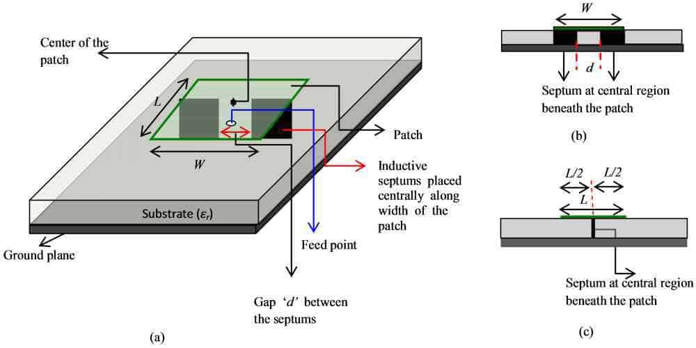
The design takes place in a way that the two metallic plates it has are placed upon each other. The antenna is then mounted or placed on a small, rectangular and flat surface.
The design iteration also has to do with the sizing of the plates. For example, one of the metallic plates, which is larger, is called the ground plane. It also has a dielectric layer in its middle.
Here is a detailed breakdown of the antenna’s structure:
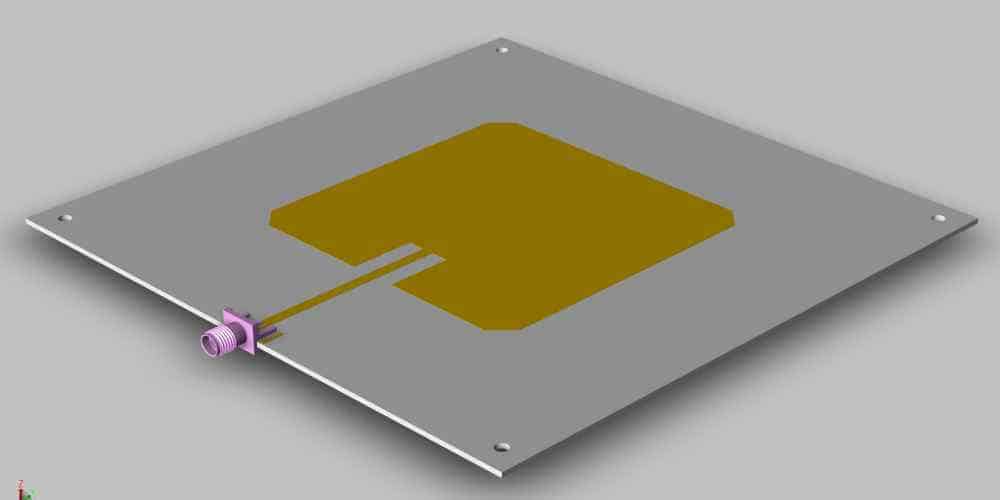
Metal Patch
This is one of the most important structures for the antenna. It has to do with the Length (L) and the Width (W). It is common to have the metal patch’s Length and Width dimensions decided by the frequency of the antenna’s operation.
The structure of the metal patch also includes the composition of the exposed trace that is either covered or protected by a solder mask, or made up of copper.
Dielectric Substrate
This has to do with the dielectric substrate that has a non-conductive layer. It helps to hold the metal patch in place.
Here are some additional pieces of information to know about the dielectric substrate:
- The dielectric substrate doubles as the substrate for the Printed Circuit Board (PCB).
- The height and the dielectric constant making up the dielectric material are usually calculated for the frequency at which the antenna is expected to operate.
The Ground Plane
Located at the bottom of the antenna (hence the name – ground plane), it serves as a conductive metal plate that is bonded to the opposite direction of the dielectric substrate.
Also worthy of note is that the plane has continuity, as derived from the continuous metal plate, which is often larger than the metal patch located at the opposite direction of the dielectric material.
PCB Patch Antenna vs. Microstrip Antenna
It is common to compare these two, but we must mention that they are almost the same. For context, the definition by Wikipedia shows that the microstrip antenna is a type of antenna, which is fabricated using the “photolithographic techniques.” These techniques are used to make an imprint of the antenna on a Printed Circuit Board (PCB).
The comparison between the two is that while the microstrip antenna is an internal antenna mostly used at the microwave frequencies, the PCB patch antenna is “an individual microstrip antenna that consists of a patch of metal foil that comes in a variety of shapes.
Important Points to Note About the PCB Patch Antenna

While you are looking to use this antenna for the circuit board design, you must also understand the place of some of the working components.
These are some of the important points worth noting about how the PCB patch antenna works:
1. Embeddable Design
This antenna owes the embeddability to the network compatibility, which bolsters the durable and robust connection. This is also the reason why the high-strength network compatibility finds easy integration into the consumer electronic devices.
2. The Ease of Configuration
You can be sure that the configuration and or design of the PCB patch antenna doesn’t require much effort. It owes this largely to the simplified polarized emission solution, which aids the operation at higher frequencies.
The ease of production is also enabled by the usage of the same type of processes and materials used for constructing the Printed Circuit Boards (PCBs), especially on a dielectric material.
3. Ground Plane Considerations
Despite the excellent performances of the ground plane, it is very imperative to take it into consideration when manufacturing the PCB patch antenna.
The core consideration here is the sizing, which in general, can be influenced by the overall size of the antenna. Due to the fact that the antenna is larger, it becomes a necessity to make sure that the ground plane’s size is made in a way that the batteries and cables connected to the device would have much negative effects on the antenna’s performance.
4. Antenna Positioning is Important
Just as we are all and about in the workings of the antenna, we must also understand the place and role of positioning. The point is that if the antenna is not well-positioned, it is possible for it to function way less than it could have.
For this reason, one of the major design factors is to have the PCB patch antenna positioned in any of the following places:
- In the corner of the PCB
- The shortened side of the circuit board and;
- At the longer side of the board.
However, if you must get the best performance, the antenna has to be placed at the corner of the board, because that is where the feed to the antenna lies in the sixth direction, while the clearance is positioned in up to five spatial directions.
5. Transmission Line Designing
The “transmission line” refers to the Radio Frequency (RF) trace that conveys the Radiofrequency (RF) energy in the PCB’s antenna. The transmission is done to aid the delivery of signals to the reception.
Here are the necessary or relevant steps that should go into the designing of the PCB patch antenna’s transmission line:
- Shortened Length: it is important to have the length of the transmission line as short as possible. The reason for sticking to a shortened length is to enable the antenna’s performance of signal transmission at a faster pace, and at the same time, reduce the losses in the cause of doing so.
- The dimensions of the transmission line should not be thin, as that potentially exposes it to losses.
6. Antenna Distancing
It is imperative to have the PCB patch antenna placed many steps away from the most important PCB components.
The core consideration is the radiation that comes from the antenna – which potentially affects the components’ performance.
These points further solidify why the antenna should be quite distanced from the circuit components:
- Keeping the antenna away from components like Ethernet cables, batteries, HDMIs, LCDs and Universal Serial Bus (USB), has a higher chance of reducing the chances of signal interference, as the signals coming from these components and the antenna wouldn’t interfere or “jam.”
- The best way to distance the antenna from the components is by taking an accurate measurement of the width and height of the components. The figure then helps you to choose the ideal positioning and spacing for the antenna.
Understanding the PCB Patch Antenna’s Feeding Methods
This has to do with the processes or techniques used when the signal received by the PCB patch antenna is to be collected. The consideration has a lot to do with the methods of feeding or inputting the signals into the antenna for onward transmission.
The following are some of the feeding methods:
- Probe Feeding: this has to do with the use of a coaxial cable to feed the signal into the antenna. It is made of two conductors – the outer connector that is connected to the ground plane and the inner conductor that is connected to the metal patch of the antenna.
- Aperture Coupling: this patch antenna feeding method deals with the sandwiching or the placement of the ground plane in-between the two dielectric materials. As a contactless antenna signal feeding method, it provides for the bonding of a feed line at the bottom side and the bonding of a patch at the top of a dielectric material.
- Line Feeding Method: this has to do with the process of connecting a narrow conductive line to the metal patch.
Conclusion: What is the Best Way to Improve the PCB Patch Antenna’s Efficiency?
It is imperative for the antenna to have a flexible connection that enables the delivery of the best results, in terms of the output.
For this reason, it is imperative to use the high-quality, Flame Retardant (FR-4) boards, as well as not using metal for the antenna’s external casing, as that limits the flow/transmission of signals.
Last but not least, the spacing of the antenna from the components is not negotiable. Most importantly, it should not be in proximity to plastic surfaces, as doing so encourages minimal losses and the dampening of the Radio Frequency (RF) signals.
