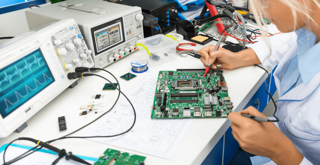
There have been several changes in the testing of printed circuits. Their ways of assembly and the techniques used for them have also been modified. These latest techs are now more feasible to make all the services related to printed circuits possible.
You will find different companies that focus on these methods in particular. Keep in mind that the production process is a bit hefty. It needs special care and precise techs for execution. The methods are reliable for the verification of the products and electronics manufactured by different producers of the electronics industry.
There are different benefits of these testing methods for PCs. These are efficient for reducing production costs. Also, enhance the quality of the circuits. It creates a positive impact on their performance later. We are going to elaborate on the PCB testing in detail.
What is a PCB Functional Testing and how to use it?
PCB testing is an important process. These inspection standards are for shortlisting the products of quality. To make sure the circuits stay true to their performance in the long run. These testing methods are important. The defective circuits never function properly. The testers for electric boards and others are for accurate inspections. There are different integral parts of these methods that need clarification. Let’s check them out below!
- Lamination: Lamination is an important factor. It is for increasing the longevity of the printed circuits. Poor lamination can damage the circuits terribly. The resistance of the laminations is directly related to their resistance against heat and forceful handling.
- Copper plating: The copper foil is for placing on the board that contains the lamination already. This will increase its tensile strength to a greater level.
- Solderability: It is important to test the ability of the solder of these circuits. The process of soldering is for combining the circuit parts on the surface of the boards. It enhances the performance of these circuits. There are different methods to test the liquid solder that cannot be ignored.
- Hole wall quality: Hole wall quality is an integrated circuit part of PCBs. The hole wall quality tells you the optimum condition of the walls. Whether there are holes or cracks in them or not. The circuits have to go through these holes. These are testing the environment and shifting of the temperatures as well. These measures are for regulating thermal stress.
- Electrical: Electrical conductivity does not matter to a large extent. The test for the electrical conductivity includes inspecting the PCB for any sort of electrical leakage to rectify it later. This test is simple.
- Environment: The operative environment for PCs are different for all sorts of circuits. Some suit humid environments, while others work with dry environments. The water absorption test is a reliable one for this aspect. The water changes in these circuits would show the ideal condition of these PCs.
- Cleanliness: Cleanliness means how well PCBs can oppose and control environmental stress. For instance, the factor of humidity is important. These PCBs are then tested under several atmospheric conditions. The experts determine what PCB performs well in a particular atmosphere, whether humid or dry.
Most Popular and Best PCB Testing Methods and Manufacturing process

1. Manual Visual Inspection
PCBA testing methods include visual inspection. The circuits need a visual inspection to see the possible defects and technical errors in them. There is a huge magnifier that clearly highlights the small parts of circuits. It makes the whole test quite feasible to conduct. This is one of the simpler testing methods.
Advantages of circuit board testing:
- This method is a basic one, and its execution is a lot easier. Simpler equipment is essential for this testing method.
- Beneficial for the huge soldering problems in circuits.
Disadvantages:
- It can be variable in results depending on the human skill.
- It is a time-consuming method and needs a huge labor power.
- It is useful for those solder joints that are clearly visible. The method is not reliable for the ones that are present at the rear side.
Applications:
It’s fruitful for those circuits that are bigger in size and work on many circuit parts in their configuration.
2. IN-CIRCUIT TESTING (ICT)
PCBA ICT is another common method to discuss PCB testing. The method is useful for inspecting the bulk production of circuits. It’s a kind of automated testing technique. It also successfully detects faults and errors for professionals. The test is useful for the inspection of all kinds of circuits, either big or small. There are different types of circuits that can be inspected with the help of this testing method easily. The testing method is recommended for those electronics that undergo defects due to soldering, wiring, and others.
Advantages:
- Detects all technical errors in a successful manner.
- Fast testing for the bulk printed circuits.
Disadvantages:
- Test jig can increase the budget for testing.
- Does not provide benefit to the prototypes of Printed Circuit Boards and their designs in terms of testing.
- It does offer a full inspection of the tester points. The testing method is only reliable for giving quick access to the tester points.
- Does not identify some faults like soldering problems and voids.
Applications: Works best to test the products manufactured in large quantities.
3. FLYING PROBE TESTING(FPT)
It’s a sub-category of in-circuit testing. It is also called flying needle testing. It’s for the enhancement of the performance of nail beds ICT. This also works well for the tester points. This testing method also deals with the vias and their issues. It also creates a positive impact on the circuit parts as well. The direction of diodes and resistors can be adjusted with this testing method easily. The measurement of voltages would also be a lot easier.
Advantages:
- Offer quick and affordable detection of faults.
- Offer full range inspection, including the testing of vias, pads, and all the tester points.
- Does not need to further add the tester points. It saves enough space on the board.
Disadvantages:
- Not reliable for bulk inspection in some cases.
- Skips out the faults like soldering problems and voids.
Application: Efficient for the inspection of prototypes and all types of circuit boards.
3. AUTOMATED OPTICAL INSPECTION (AOI)
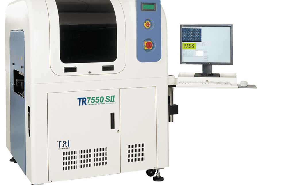
AOI includes working with two/three-dimensional professional cameras that function well due to high resolution. These cameras are for getting HD images of the small circuit parts. So that their inspection would get a lot easier with clear visualization. The AOI machine also offers quick inspection on all counts.
This method is open to making quick fixations and changes. There are little or no restrictions for this method. It also works well with a visual inspection which is a simpler method. It is for making sure that the circuit boards are precise and persistent in their performance. You can also use this method to inspect the part of the wrongly positioned circuit to adjust them. The method offers a higher degree of precision. The designs and prototypes of circuits don’t go well with this method at all.
Advantages:
- Excellent for solder joints inspection.
- Works more efficiently than basic human inspection methods.
- The technicians can rely on the method for initial inspection after the production process.
Disadvantages:
- AOI does not provide inspection on a deeper level.
- Time-consuming process for the designs of PCBs.
- Database matching is not a hundred percent precise for reliance.
Application: Dependable on testing the products manufactured on a large scale.
4. AUTOMATED X-RAY INSPECTION(AXI)
It is a reliable method and uses x-rays for inspection. These go through the object and produce HD images of the object for the users. The tech works in an identical way for the solder joints as well. Also, the method is essential to unleashing the hidden solder joints.
Extremely helpful for the identification of any voids and other problems if there are any present. It is important for the initial detection of technical faults. The process is for saving the inspection cost for the producers. The method is reliable for a small-to-medium range of products in terms of inspection as well.
Advantages:
- The detection rate is way more than other testing methods available.
- Focuses on the prolonged performance of the solder joints.
Disadvantages:
- Highly trained and skillful technicians are important to execute the method.
- Not an affordable process and is also time-consuming.
Application: It’s a befitting method for chip inspection on a large scale along with printed circuits.
5. BURN-IN TESTING
The burn-in testing is another type of testing method. It’s reliable for the quick and precise inspection of irritating faults in printed circuits. This method is for enhancing the performance of the printed circuits under extreme and stressful conditions. The method is also crucial for the testing of PCs in terms of load capacity.
So that the odds of failure of these circuits would be minimized to zero. The method is reliable for the testing of common faults of the printed circuits. These conditions might be voltage stress and frequency of operation that must be tested with a reliable method. The data collection is important for future decision-making for professionals.
Advantages:
- Real-time checking of PCBs in stressful and challenging environments for them to function.
- More product quality and effective durability.
Disadvantages:
- The testing method can create a negative impact on the product due to its long duration.
- Takes a lot of time for the entire execution.
Applications: Essential method for the electronics that are used in the domains of defense and military.
Why PCB tester and testing is essential?
Testing is a crucial part of the production of printed circuits. There are different steps in the production of PCBs that need persistent testing methods. Therefore the shortlisted printed circuits can be shipped to their order destinations from the production firm.
There were former testing methods quite common in the old days. These would automatically reduce the technical faults as well. These are viable tests for the prototypes and easy PCB assembly.
Amazing Benefits of PCB Testing
The benefits of testing methods of PCBs are no less. These benefits would make the entire production and usage of PCBs outstanding for both parties. Let’s learn bout these benefits below!
- Bug identification: The bugs and errors would be identified easily through testing and inspection. This would enable the functioning of the circuits for the users by all means possible. All the issues related to production can be rectified later due to early inspection.
- Time savings: The testing is also beneficial in terms of early inspection of the layouts and prototypes of the PCBs. So that there would be fewer chances of any kind of technical error in the products; this helps in the fast initiation of the production process. Since the technicians would identify and correct the faults in prototypes of PCBs with testing.
- Cost reduction: You can easily avoid wastage in terms of assembly through complete testing. Also, the technicians would save labor costs with the help of timely product inspection. The companies can also remove the faulty circuit parts once they get identified with testing methods. Therefore cost reduction is an important benefit of the testing methods.
- Fewer returned products: The company can face a huge loss when the customers return the products. This can lead to lesser revenue generated for the company. With the help of testing methods, a company can reduce the chances of product returns, thus leading to more revenue generation for the company. Another essential benefit of testing methods.
- Increased safety: There are many circuit parts that can be harmful and unsafe for users. So thorough testing would exclude this risk as well. The products and the printed circuits would be safer for reliable usage, which is an important factor that is beneficial due to the suitable testing methods.
There is no doubt that some of the testing methods are much more exhaustive. These are not easy at all. However, some sorts of printed circuits don’t need extensive testing techniques. There is still a need for testing methods for some printed circuits that would improve their performance and longevity. Therefore companies must learn and dig deeper into the benefits of transparent testing methods for the printed circuit. So that safe and quality printed circuits would be possible to supply to the consumer base.
