AT&S PCB is a good choice when it comes to modern applications. The company produces world-class PCBs and also IC substrates which are quite common and crucial these days. The shipping is operational around the globe. The company functions in Asia and Europe.
It has different partners in many regions .. One of the best parts about the company is that it is good at providing well-performing technical products to its customers. These products are related to the domains of computer electronics, communication, medicine, industry, and mobility.
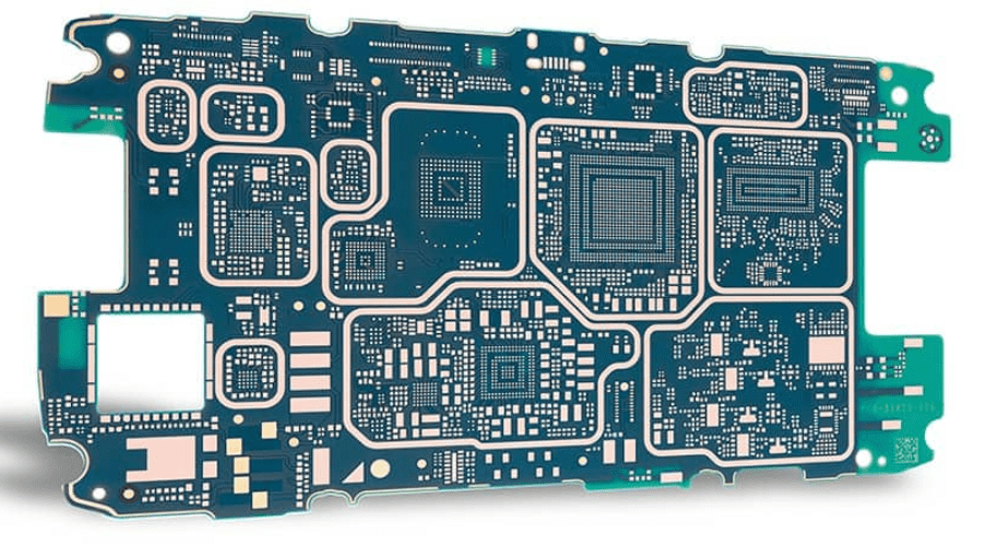
AT&S Packaging of PCB And Advanced Technology Inventions
The forum of Red Bull Ring usually houses racing cars usually run laps. The execution of AT&S led to the discovery of the latest trends in PCBs and the rectifications related to them. The forum also imparts knowledge in the form of a comparison between these two domains.
In terms of speed, high efficiency, reliability, and technology. Interested people can learn about the progress of the PCB domain by getting familiar with the integration of PCBs in mobile devices, automotive systems, and industrial, communication, and medical technology. The PCB has also found its applications among the gadgets which run on 5G.
The process of miniaturization is an important aspect of PCBs. It gives rise to projects based on their research and progress. During this phase, the key aspects are modern methods of packaging and effective solutions for more heat dissipation in the case of intense and complicated PCBs.
5G Mobile Communications
The study also included shedding light on communication of 5G mobiles and their usage for testing the virtually assembly of circuit boards and ECPs). Also, experiments were conducted to manufacture PCBs with 40-50 layers and even more.
The PCBs are important for 5G communication because of the reasons like enhancing needs of data rates and signal-based integrity. The automobile sector also predicates PCBs to a large extent in terms of driving and electromobility. However, there are some major setbacks to attaching 5G in such machinery. These include higher integration density, more losses in signals, high frequency, and thermal management.
AT&S teams up with 5G to give birth to integral technologies of the present and future. These include substrate such as circuit boards and mSAP. The goal is to enhance the functional integrity along the z-axis in case of small to medium heights.
It results in impressive signal integrity and better management of thermal. Filters and antennas are HF circuit components and are cost-efficient at the same time. This technology is also beneficial for incorporating management of thermal mechanisms such as heat pipes or plates of copper.
Thermal Management
The trend of miniaturization is accelerating at an unbelievable pace. Due to this sole reason, it is important to sustain thermal management. To do this, thermal resistance has to be alleviated.
The factors like surface area, which is larger the better, conductivity, if higher, the better, and the heat transfer path should be kept short always. One cannot neglect the important thermal contact points. AT&S has the ability to cope with the problems of thermal management and relevant processes. The solutions offered by this technology are laser vias and insulated metal substrates (IMS).
High-Power Devices
Along with copper inlays or 2.5D technology with cavities. In forthcoming years, this will also help with the phase-change materials (PCM) that would be attached to the hot regions.
It is the best possible way to deal with high-power devices and applications that would work equally well, even if they gather little room. It is also beneficial for power density. The requisite is to devise ways to deal with the heterogeneous packages to improve their functioning and durability.
There have been cases when the prototypes failed due to the copper migration. To solve this, AT&S offers a product-independent leakage testing vehicle (LTV). The benefit of it is that it expedites the process and executes fast analysis and correlation.
Some other benefits of LTV are detecting errors in the analysis, identifying the leakage, and conducting material investigations, which are essential. It also supports working with simulation tools to enhance work efficiency.
AT&S PCB Combats Energy Losses In Microelectronics
The role of energy consumption by microelectronics is huge. Big and powerful electronics need a persistent and large source of energy all the time. Otherwise, they would fail to work properly. AT&S is an effective way to either increase the energy supply or reduce its requirement or demand for electronics.
The company has claimed that it is working with its teams in different regions . and shakes hands with ‘The Centre for Power Electronics Systems of Virginia Tech (Blacksburg/Virginia). It is among the largest markets of electronic appliances and functions as a research facility in the development of this kind of technology that stabilizes energy distribution.
CPES
The domains of research are generally revolving around microelectronics and battery-powered vehicles to regional and national electricity distribution systems. CPES takes great pride in standing five impeccable universities and many enterprises on the basis of IPEM (Integrated Power Electronics Module). The energy distribution is a major crisis in the world. Things need to be done in time to deal with this setback that can disrupt major sectors of electronics.
CPES is a great partner in terms of research and implementation. It has devised various solutions to manage the problems related to energy distribution. Also, major energy sectors are gaining boons from the offered and existing solutions. The aim is to give rise to such technologies that would alleviate the need for energy in the field of microelectronics so that the energy crisis would be addressed in a successful manner.
IC Substrate
One of the important IC substrates is a translator between the micro parts of the PCBs and microchips. These are commonly useful in powerful computers. The IC substrate manufacturer, which is located in Lebanon, designs these substrates in a remarkable way. These have the ability to lower the need for energy usage by the microchips, and there is a considerable reduction of energy during the process of data transmission too.
