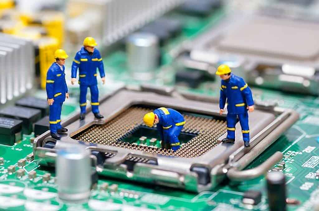
Before you can repair a PCB, you must first determine what the problem is. Professional repair teams usually have a power or voltage meter, which they use to diagnose electrical problems on the board. This tool is essential when diagnosing a problem on a board with no visible damage. A professional repair team will also use special tools to perform the repairs. The repair process generally involves reseating the components.
What Causes PCB Failure?
One of the most common causes of PCB failure is heat and humidity. Different materials have different coefficients of thermal expansion, which can cause constant thermal stress, weaken solder joints, and damage components. To avoid these problems, design decisions should prevent thermal stress.
Another critical factor is the operational environment. While PCBs can handle a range of temperatures, extreme temperatures can cause significant damage. To avoid PCB failure, keep the working environment at a moderate temperature and use good ventilation techniques. Also, avoid using PCBs around liquids or flammables.
Other common causes of PCB failure include manufacturing defects. While we can prevent some of these defects during design, others are difficult to correct or prevent once they’ve occurred. For instance, we may discontinue solder joints due to misalignment, which can lead to malfunctioning components. Similarly, improperly placed mounting features or components may also cause PCB failure.
Despite the many risks, it’s essential to remember that there are several preventative measures to avoid PCB failure. One of these measures is to use lead-free solders. Lead-free solders require higher temperatures, and improper soldering techniques can result in faulty PCBs.
Repair process
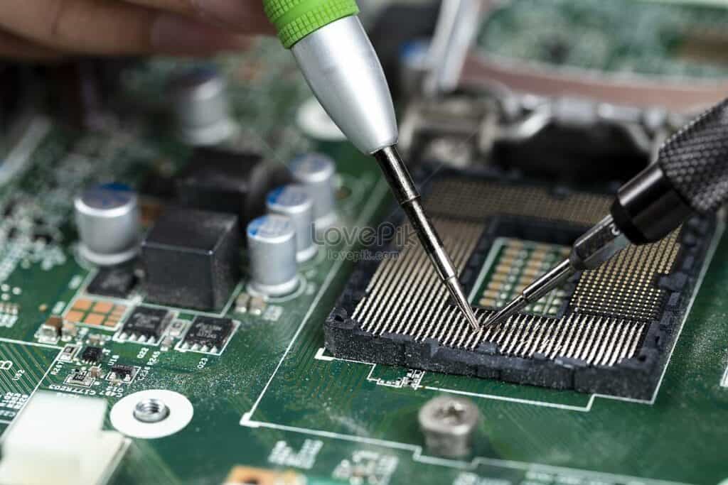
Reballing or resoldering
If you’re looking to reball or resolder a PCB, there are a few simple steps to follow. First, clean the old solder paste from the ball pads using a chemical cleaner. Then, apply new solder paste on the pads using a paste dispenser. Finally, remove any old capacitors, resistors, and ICs from the PCB before reballing.
Reballing or resoldering is a labor-intensive process, and it requires a considerable amount of practice. You cannot learn the process in a week, so you must practice constantly until you become adept at it. Fortunately, there are many tools and resources available to help you.
A PCB may need to be reballed because solder bridges may have broken or delaminated from the surface. This could prevent electrical current from flowing or cause the circuit to malfunction. This procedure is not simple and requires several tools and supplies, but it can yield a significant result if done correctly.
If the soldering iron doesn’t remove the entire solder, try placing solder balls in the holes. The solder balls will fill in any small holes, but you may still need to heat the chip holders to ensure all the solder has melted.
Micro-abrasive blasting
Micro-abrasive blasting is a process of cleaning and repairing parts by removing surface layers. Its effectiveness depends on a few factors, including the abrasive, the nozzle, and the pressure. A micro-abrasive blaster can also help to deburr or cut surfaces.
Micro-abrasive blasting uses natural abrasives, such as nutshells and fruit kernels, to remove coatings without causing damage to the underlying material. The process does not require solvents, which minimizes the risk of contamination. It also reduces static electricity, which can damage PCBs.
Even though the process is effective, it can cause problems. For example, when soldering, contamination from the soldering iron can cause dendritic growth, resulting in a board failure. Another common problem is corrosion caused by salt in the air. When this happens, the solder can pop off the traces, resulting in a short circuit.
Before attempting to repair a PCB with micro-abrasive blasting, ensure the board is unplugged from the power source to avoid any potential electrocution risks. It is also essential to ensure that supplemental batteries are disengaged.
Micro-abrasive blasting can remove adhesions and coatings and can be used to remove conformal coatings. The cost of micro-abrasive blasting equipment depends on the equipment used. Some units are free and cost less than $5k, while others cost more than $13,500.
Overcoat Pens
Overcoat Pens are an excellent way to repair PCBs and other electronic components quickly. Squeeze the barrel and press the tip to dispense conductive ink onto the break area. This product dries tack-free in five minutes and cures completely in 30 minutes. Heat-curing is also an option if necessary.
Overcoat Pens can be necessary on the soldered connections on PCBs. The clear overcoat pen is ideal for small areas, and we apply it by pressing the tip against the board. For larger areas, we can use an acid brush. Use caution around connectors; one should cover with a temporary solder mask or Kapton tape. Copper tape melts very quickly and may corrode the connectors, so use this material sparingly.
Overcoat Pens can also be helpful for solder mask repair. They help protect sensitive electronics from arcing and moisture. In addition, they can provide a protective shield against fungi, moisture, and abrasion. Finally, if we expose the PCB to abrasive material, an Overcoat Pen can prevent this and ensure proper protection.
Overcoat Pens are easy to apply and are a great way to repair a PCB. They are a modified acrylic conformal coating. The only downside of Overcoat Pens is that they will break down at higher temperatures than epoxy. This is why it is essential to apply this product only after soldering. In addition, it will protect the circuit traces from arcs and shorts and static discharges.

QC fault labels
The placement of QC fault labels on a PCB is crucial for proper debugging. You should place labels so that the reader can quickly determine the attribution of the label, and they should not cause any ambiguity. If the labels are not in the correct position, a PCB can be severely damaged or destroyed due to a QC fault.
Printed PCB labels can provide a high level of traceability. They also help manufacturers improve their management capabilities and increase production efficiency. However, they must ensure long-term readability and durability. Otherwise, manufacturing errors may occur. To ensure this, labels consist of durable materials.
Test points are small areas of exposed copper on a PCB that can be connected to an oscilloscope probe during development or to a contact pin during production. Usually, these test points are on the bottom of the PCB, but more complex boards may have test points on both sides. Most PCBs require at least one engineering test. Using meaningful labels makes the testing process much easier. Furthermore, numerical test point references are helpful during debugging.
PCB fault labels can consist of a variety of materials. Each type offers different levels of durability. For example, polyimide labels are ideal for the beginning of the manufacturing process, as they feature temperature-resistant adhesives and substrates. These labels can withstand high temperatures during wave soldering and reflow processes. If the labels need to remain intact after washing the board, you should use polyester PCB labels. These labels can withstand IPA cleaning chemicals.
Cleaning flux residues
There are several factors to consider when cleaning flux residues on a PCB. First, you must choose the right cleaning chemistry. This should match the amount of flux and the cleaning process you are using. You should also validate the cleaning method by conducting testing, ionic testing, and other methods to determine the level of residue removal. These steps can reduce costs and increase the reliability of your PCB.
Secondly, you should ensure you clean the soldering flux on the board. This is because flux residues can cause problems for your PCBs, such as reducing the life of components. If the board remains without cleaning, it can lead to corrosion and shorting between circuits. Ideally, you should clean the board both before and after soldering.
Flux residues can be a problem when you’re working with high-end electronics. They can cause corrosion, swelling, and even failure. It’s critical to clean the PCB to avoid this, especially if the electronic components are very sensitive. Even a small flux can cause problems, but you should clean it thoroughly before putting it back into a product.
Next, you should clean the components with a flux cleaning solution. You can either use a brush with a trigger to scrub the board thoroughly or use a spray bottle. In either case, you must ensure that your brush is soft and flexible to avoid damaging delicate electrical components. Afterward, you should apply the solvent to the board using a spray bottle or toothbrush. The solution will soften and dissolve the residues. During this process, you need to be patient and use gentle pressure.
Using a voltage meter
Using a voltage meter is an excellent way to diagnose a problem. For example, when troubleshooting a broken PCB, you can use a multimeter to help you make sure that the problem is a single component rather than a system. You can use the multimeter’s probes to test for resistance and continuity. The red probe should connect to the cathode of the PCB, while the black probe should connect to the anode. The multimeter will indicate a low resistance when the probes come into contact. If there is an overload indication, the meter will display the digit “1”. If you cannot identify a single component, you can use a multimeter to test for the continuity of other components.
The meter will measure the voltage and current between two points, and the voltage reading will be proportional to the current. Therefore, if you see any more current than 200 mA, the voltage is too high, and you should repair the PCB needs. However, if the voltage meter doesn’t measure the current, it will give an inaccurate reading.
When using a voltage meter to repair a board, you can set the range dial to either AC or DC voltages. Selecting the right voltage range is essential, as the voltage may vary between AC and DC.
Safety Measures When Repairing a PCB
When repairing a PCB, it’s essential to use proper safety measures. For example, leads and solders can splatter, and wearing safety glasses is crucial to prevent any possible eye or face injuries. It’s also essential to avoid electrostatic discharge, which is a common problem in electronic devices. This phenomenon occurs when there is a significant electron difference between a PCB’s surface and another object’s surface. Using an ESD-free mat or a grounded wrist strip can prevent this problem.
