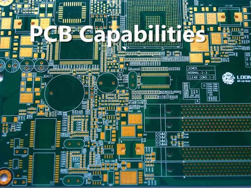
PCB Capabilities
PCB Technology is changing very fast,Every year new technology or new machines join PCB manufacturing,If you doubt your design that can manufacture or not ,Send emails to sales@raypcb.com,We love to give some suggtions basing on the lasting production process .
1. Max Layers: 1 to 56 Layer PCB
2. PCB Raw Materials:Fr4,Rogers,Aluminum,Copper,Cem1,Teflon,Taconic,Arlon,Isola (Mixed Lamilate is accepteable like:Fr4+Rogers Material)
3. Max Panel Size : 600*770mm( 23.62″*30.31″) for long PCB board one side can be 1500mm .
4. PCB Thinkness: Rigid PCB – 0.1mm -5.6mm Flex PCB:0.1 -0.3mm
5. PCB Hole Size: Min 0.15 by drilling , Min 0.1mm by Laser
6. Min Line Width/Space : Rigid PCB – 3mil/3mil , Flex PCB 2mil / 2mil
7.Inner /outner Copper Thickness : Max – 6 oz/10 oz
8.Solder Mask Colors: Green,Black,Blue,White,Yellow,Red,Purple ( Mixed colors is acceptable like Top green bottom white ) Peelabe Solermask is welcome .
9.Silkscreen Colors: White,Yellow,Red,Black
10.PTH Hole Tolerance : ±0.076mm(±3mil) (Request pressfit hole :≤±0.05 )
11.Non-PTH Hole Tolerance: ±0.05mm(±2mil)
12. Hole Copper Thickness: 20um normall , 25-30 is available .
13.Min Solder Mask Pitch : 0.1mm (4mil ) (Solder Mask Bridge 0.1mm)
14. Min Inner Layer Clearance : 3 mil
15. PCB Impedance Control: 1×10¹²Ω(Normal) Control Tolerance : +/- 10%
16.PCB Warp and Twist Control: ≤0.7%
17.PCB Insulation Resistance : 1×10¹²Ω(Normal)
18.PCB Through Hole Resistance : <300Ω(Normal)
19.PCB Thermal Shock : 3×10sec@288℃
20.Test Voltage 50-330V
21. Outline Tolerance : ±0.15mm ±6mil
22. Outline Methods: Routing,V-Groove, Beveling punch
23. PCB Surface Process : OSP,Hasl,LF-HASL,Immersion Gold(ENIG), Immersion Silver,Immersion Tin,Plating Gold (Hard Gold) ,ENEPIG (NI/PA/AU)
24. Others: 1.Countersink Hole 2.Carbon Oil 3.Half Hole 4.HDI (Blind and Buried any layer connect)5.Rigid Flex PCB
25. Standard: IPC II / IPC III , Military Grade
