If you’ve ever wondered what Immersion Tin is, you’ve come to the right place. Read on to learn more about the process. What do you understand by the term Immersion Tin. Why do we use Immersion Tin? And what steps are essential? In this article, you’ll learn more about the process and why it’s so popular. You’ll also learn about the benefits of Immersion Tin.
We will discuss the Immersion tin PCB features and advantages and how to perform this process. We’ll also go over some of the disadvantages of Immersion tin, and what it can do for your products. In addition, we’ll look at how Immersion Tin is a great option for BGA and fine pitch surface mount components. The best part is that you can do it yourself, so you don’t have to hire a professional.
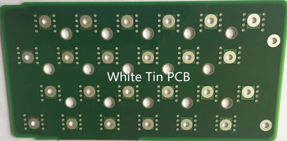
What immersion tin plating means
Immersion tin plating is a metallic layer deposited on the copper surface of a printed circuit board. It yields a consistent thin tin layer on the copper surface of a printed circuit board. The coating is 0.8 to 1.2 micrometers thick and has good hole wall lubricity. This process is self-limiting, as the process relies on a chemical reaction between Copper and Tin.
The chemical process occurs only in the presence of the carcinogen thiourea. Therefore, high levels of control are necessary to ensure that the metal deposits properly and uniformly. It is possible to accomplish it through bathing the PCB in your electroless chemical solution. Such a process protects copper layer against oxidation thus extending the shelf life when in storage. The tin layer formed is whitish on completion of plating process.
Immersion tin plating involves dipping a circuit board in a copper and tin ions solution. This step speeds up the electroless reduction process, where there is formation of a thin layer of tin metal on the copper pads. However, one must carefully monitor the solution’s composition and temperature. The PCB will become turbid and unsuitable for use without the appropriate composition. Fortunately, this process does not require any chemical cleaning after the plating process.
What is tin plating solution?
Plating copper on PCBs is now possible with the help of chemical immersion tin. This process does not lead to contamination and does not produce a polyester layer on the solder mask. You can apply tin to any hole size or position on the connection plate. A lead-free version of immersion tin is also now available. This process is a prerequisite for DPMC’s development plan.
An immersion tin plating solution is a re-usable solution that deposits tin onto copper traces on a circuit board. Professionals call this process immersion tin plating and reserve the term electroless for something else. The solution can plate 1.0 to 1.5 microns, depending on the size of the part to undergo plating. However, the tin deposit is not very large, and the solution will become very turbid if it does not contain hypophosphite.
Features of Immersion Tin
The surface finish of an immersion tin PCB is highly sensitive and requires careful handling. It may face damage when not handled properly, resulting in short circuits and poor solder joint quality. It can also affect the overall performance of a circuit board. As with any circuit board material, there are advantages and disadvantages to immersion tin plated PCBs.
The process of immersion tin is similar to that of Imm Ag, but differs from it in several ways. In the first instance, the process requires immersing the circuit board in acidic solution to remove surface impurities.
Process of tin plating by immersion
In tin plating, there is the use of a bath composition containing a soluble stannous salt, sulfur component, mineral acid, and wetting agent. The bath formulation is essential to deposit an even coating of tin on metalized surfaces. This plating method is advantageous because it can deposit up to 300 millionths of an inch of tin metal. In addition, the resulting coating provides good solderability immediately following plating and after adverse conditions.
Tin whiskers appear when the surface of the coating is exposed to external stress. A Ni underlayer, deposited between the immersion tin surface finish and the Cu substrate, mitigates the effect. Researchers should study the effect of stress distribution on tin whisker growth. For this, a quantitative analysis of the stress distribution should be performed.
Advantages of Immersion Tin PCB
The advantages of immersion tin PCB over other surface finishes include the ability to produce white surfaces and a reduced cost. In addition, the PCBs are compatible with fine pitch components. They are also free from black pads. This is a relatively inexpensive surface finish that is well-suited for high-volume manufacturing. For more information, contact a PCB manufacturer.
Immersion tin PCBs are ideal for many different market segments. The tin layer is uniform and thin, and the process protects the copper layer from oxidation. It also prolongs the shelf life of the printed circuit board.
Also known as White Tin, immersion tin is the most cost-effective surface finish method available. It is RoHS compliant and provides excellent planarity. In addition, its application requires less water and chemical, making it a popular choice for budget-minded PCB manufacturers.
Disadvantages of Immersion Tin PCB
Immersion tin PCB is widely used in communications PCB boards, but has certain disadvantages. For example, it is not as solderable as other printed circuit board materials and the surface finish can be damaged by improper handling. In addition, immersion tin PCB can suffer from poor solder joints and may cause short circuits.
In terms of price, immersion tin is the cheapest PCB surface finish. However, it has a limited shelf life because of the use of a chemical called Thiourea, which is a carcinogen. In addition, immersion tin is also less environmentally friendly than immersion silver. However, unlike immersion silver, it can stand multiple reflows and has a longer shelf life.
It is difficult to solder tin-coated PCB. While immersion tin PCB is more expensive than lead-based PCBs, it’s more affordable than other PCB materials. The copper surface is less susceptible to oxidation. However, it’s also more fragile and prone to cracks. Immersion tin is applicable for sensitive components like ICs and BGAs.
The Advantages of Electroless Nickel Immersion Gold (ENIG) For PCB Manufacturers
Electroless Nickel Immersion Gold (ENIG) is a type of surface plating that covers electroless nickel with a layer of immersion gold. This highly reliable process provides a very planar surface with an excellent solder joint. Because it is highly resistant to environmental conditions, ENIG is applicable on all types of PCB configurations. In contrast to HASL, ENIG is more expensive than HASL, but it offers superior characteristics for printed circuit boards.
Several design advantages characterize ENIG processes. First, because they use different chemistries, they are gentle and do not require frequent dummy plating. In addition, you can associate ENIG processes with a long dwell time in an electroless nickel or immersion gold bath. These characteristics make ENIG an excellent choice for parts that need to be extremely sensitive or delicate.
In addition to the quality and performance of the finish, electroless nickel plating can help reduce the cost of production. Because the surface of the copper substrate can become porous, it is crucial to choose a gold process that can prevent this issue. Black Nickel is difficult to detect and can affect the integrity of a part. There are several root causes of this issue. For instance, it can occur when the copper surface is not smooth, or when the immersion process is too aggressive.
Which PCB Surface Finish Is Right For Your Next Project?
Before deciding which PCB surface finish is right for your next project, you should consider cost and turnaround time. Contract manufacturers have turnaround times as quick as 3 days and can give you an accurate quote in as little as a day. Contract PCB manufacturers emphasize design for manufacturing and source all components from the finest suppliers. In addition, they perform multiple automated inspections during assembly and provide support for the entire printed circuit board (PCB) manufacturing process.
Immersion Tin VS Immersion Silver Finish
When comparing the costs related to PCB surface finishes, immersion tin vs. immersion silver, the latter’s cost is the first consideration. Immersion tin is inexpensive, easy to fabricate, and does not require a complex assembly process. This PCB surface finish method is also a cost-saving option, as it provides a flat surface for mounting PCB components.
While there are many advantages to immersion tin and immersion silver, the former may be better suited to many applications. PCB manufacturers should consider their performance requirements, material cost, and budget when deciding between these two surface finishes. Immersion silver is generally less expensive than HASL, which might be tempting for a company trying to meet RoHS compliance. But immersion tin carries its own risks.
However, while both are environmentally friendly, immersion silver is more susceptible to temperature, humidity, and handling. As a result, it requires extra care.
Immersion Tin VS Immersion Gold PCB Surface Finish
The immersion tin is more affordable and easy to fabricate. It is also a more environmentally friendly option, and both are inexpensive. Immersion tin is good on press fit pin insertion and backplane applications. Its benefits include good solderability, oxidation resistance, and intermetallic diffusion.
Immersion tin PCBs have a shelf life of three to six months.
What is Immersion Tin PCB Thickness?
When it comes to circuit boards, one of the most important considerations is the depth of the tin layer. During this process, a liquid bath containing Tin cations is used to deposit a thin film of tin onto the PCB. The resulting layer is between 0.7 and 1 micron thick.
Immersion tin PCBs are reliable for press-fit pin insertion, but they may lose their solderability after several thermal cycles. This is because tin and copper are chemically very similar, and diffusion will occur over time, which will reduce the solderability. The surface finish is also sensitive to handling and can cause the board to tarnish or develop tin whiskers, which can create short circuits.
Is immersion tin lead free?
Increasing concern about the environmental impact of lead is driving a transition in surface finish technology away from HASL to other lead free finish options. The most common alternative to HASL is immersion tin plating, which offers many advantages, including low deposition costs, good solderability, and compatibility with existing lead-free assembly processes. But what about the lead free finish aspect of immersion tin plating?
Immersion tin has two distinct advantages over hot air solder leveling: it supports rework of the solder joints and has a high tolerance for oxidation and corrosion. It also provides a thin, flat surface for soldering. The thickness of immersion tin is typically between 1.3 and 1.15 um. The first step in the process is to dip the circuit board in acidic solution to remove surface impurities. You then wash the circuit board using water to eliminate the cleaning solution. This step improves the plating process efficiency. While the immersion tin process is not entirely lead free, it is compatible with a wide range of applications.
PCB Lead Free Alternative
If you’re looking for a printed circuit board lead free alternative, you’ve come to the right place. If you’re using lead-free solder, the first step is to find a lead-free soldering alternative. While it’s tempting to use the same lead-free soldering agent that you use with lead-based solder, you should remember that a lead free alternative will usually require higher reflow temperatures, which can cause warpage and stress on printed through holes.
RoHS regulations have had a huge impact on the manufacturing of printed circuit boards, and the process of PCB assembly must comply with the new rules. Lead-based solders, traditionally used in printed circuit board assembly, must undergo replacement by lead free alternatives. There should be the elimination of other substances such as cadmium and mercury as well. By using a lead-free alternative, the PCB process becomes more efficient and environmentally friendly. Lead-free PCBs are a great way to attract customers who value environmental protection and eco-friendly manufacturing.
