PCB IMPEDANCE
Every PCB has an important parameter called Impedance(Z) which is ranging from an average of 25 to 120 measured in ohms. It is the combination of capacitance and inductance in an Alternating Current(AC) characteristic dependent on frequency. Being said significant, certain digital applications utilizing higher frequency require controlled impedance in measurement be within a regulated range with tolerance to maintain data integrity and signal clarity.
CONTROLLED IMPEDANCE DESIGN GUIDE
Controlled impedance PCB benefits to repeatable high-frequency performance having no reflection. One of which is a transmission line that is formed by PCB conductors having controlled impedance propagating without distortion. It is characterized by physical factors: dimensions and electrical characteristics of the conducting and insulating material of the circuit for impedance matching. In addition, the design of the PCB layer structure composed of the copper line width, routing features and others affects the impedance of the PCB. There are also multiple practices in manufacturing and design that affect impedance of the circuit. Further will be discussed below.
PCB MATERIAL PROPERTY AFFECTING IMPEDANCE
The following are properties of materials affecting impedance of the circuit
- The Dielectric Constant of the Insulating Material
The insulated material is also called the substrate which is the board itself. It serves as the electrical insulation between the conductive parts. It has a property called dielectric constant which is the ratio of the capacitance of the material to the capacitance of an ideal capacitor. But in the technical practice of frequency under 1Mhz, it is measured and not calculated since the same PCB material differs in properties in manufacturing due to resin content.
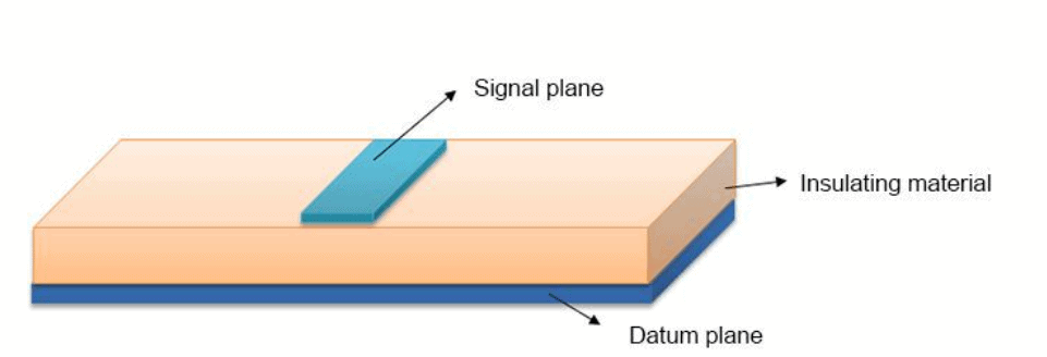
Figure 1. Insulating Material
The operating frequency is determined by the dielectric constant of the insulating material. The lesser the dielectric constant, the higher the resulting frequency and the higher the characteristic impedance resulting in faster transmission of the signal. It is highly preferred to use a material with a lower dielectric constant (DK) to ensure the best signal performance and minimizes any signal distortion or phase jitter of the signal. Below are dielectric constants of the some oftenly used substrate.
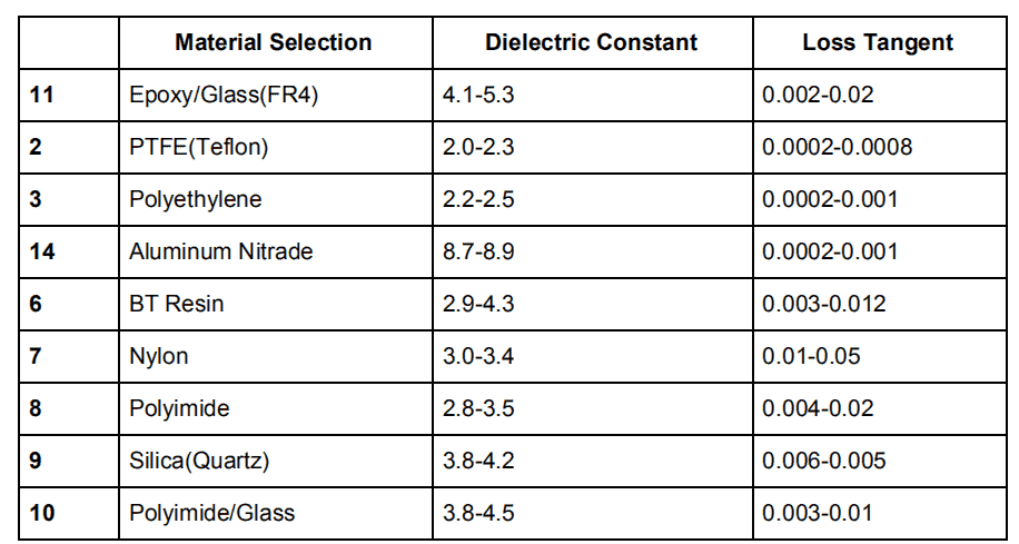
Table 1. Material Properties2. Lower Loss Tangent Material
The dissipation factor is another term for loss tangent. It is the measure of signal loss as the signal propagates through the transmission line. The higher the needed Impedance for high-frequency applications, the lower loss material should be used. Table 1 shows loss tangents of the some oftenly used substrate.
- Thickness of Insulating Medium
Characteristic impedance is directly proportional to the height of insulating material. Since the trace width, copper thickness and dielectric constant are determined prior to the manufacturing process, height of insulating material is the factor that primarily controls the characteristic impedance in the manufacturing process through adjusting the lamination thickness. An increase in 0.025 mm of the thickness increases the impedance by 3 ohms. Since the thickness of the laminating material is adjusted during the production, some tolerances are considered for ease of manufacturing.
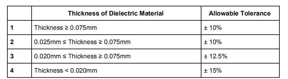
Table 2. Tolerance of Insulating Material4. Fiberglass weave pattern for PCB Core
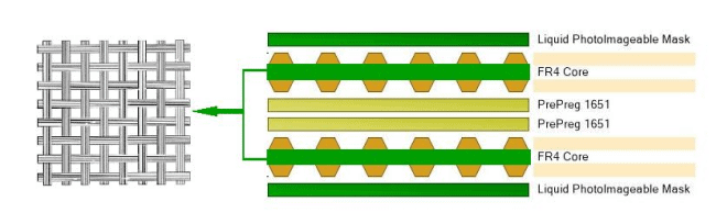
Figure 2. PCB Core Weave Pattern
Since dielectric constant is inhomogeneous across the sheet cores, using a woven fiberglass style for the PCB core improves it across the materials for better controlling impedance, less power degradation, and avoids signal issues especially for High-frequency signals (>100MHz). A tighter weave pattern causes more uniform dielectric constant throughout the PCB.
B. CONTROLLED IMPEDANCE PCB LAYOUT RULES
The following are layout design considerations achieving controlled impedance by preventing problems related to Electromagnetic Impedance(EMI).
- Width and thickness of the Copper Line
A dramatic change of PCB impedance is caused by a dimensional change in trace width. An increase in impedance of 1ohm has resulted from a trace width increased by 0.025mm. While on the other hand, the trace thickness, which on average is 25μm, is composed of copper foil plus coating.
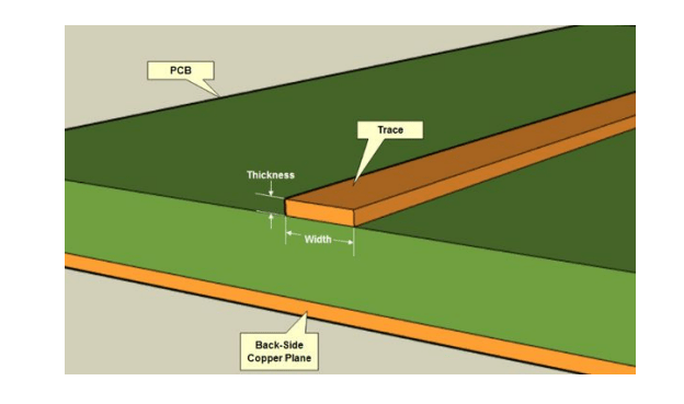
Figure 3. Trace Width and Thickness
By simply varying these dimensions, expectations of demands of current capacity and better thermal capabilities are satisfied.
2. Traces Crossing Split Planes
To prevent increasing impedance, making PCB prone to interference with others, and to avoid signal degradation, copper lines should not be routed across a split plane. Delay in signal propagation also happens due to increased series inductance. And this kind of design minimizes the current loop area in the return path along with any impedance discontinuity created by crossing the split plane.
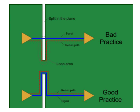
Figure 4. Traces Crossing Split Planes
If avoiding traces to cross split planes is not doable, a solution of stitching capacitors across split planes can be routed over it. An exemption can be made if the design objective is to have increasing impedance.
3. Traces with no Reference Ground Points/Planes
Providing a complete ground reference plane on the adjacent layers is necessary either on the top or the bottom layer. Without this, its impedance will be unacceptably high. The connection has to be direct from the component to a ground point in the circuit to ensure low impedance.
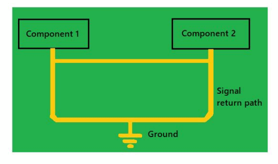
Figure 5. Common Ground Points
Different types of impedance are affected by common ground points/planes. One of which is Ground Impedance. By having a common ground plane, the ground impedance is significantly reduced. This also serves as a tool to combat crosstalk. Second is the impedance of current return paths. It is the path where the current takes to return to the source. By using a ground plane, impedance is minimized.
4. Mismatches in length
Groups of single-ended impedance traces are uneven lengths between differential pairs. This should be avoided to prevent signal distortion and increase the bit error rate. There is a tolerance of +/- 5 mils between the differential pairs.Reducing the lengths of traces should be done to prevent reflections by proper termination.
- PCB Line Spacing
Common prevention of flashover or tracking between conductors is having spaces between them. For the Impedance application, the good dielectric spacing between the copper achieves a consistent electrical performance of the PCB.
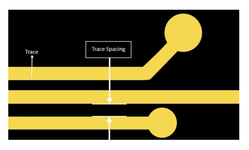
Figure 6. PCB Line SpacingC. PRACTICES CONSIDERATION AFFECTS PCB IMPEDANCE
- Use of Back Drilling
In some cases where the signal goes from a top layer to an inner layer using thick backplane results in reflection since there is excess copper upon applying copper barrel. By using back drilling, the unwanted copper is removed.
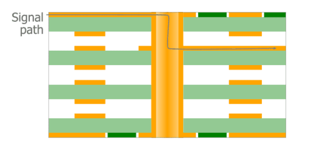
Figure 7. Back Drilling
By using back drilling, signal attenuation is reduced due to improved impedance matching.
- Avoid Thicker Solder Mask
As the thickness of the solder mask increases, its dielectric constant as well increases which inversely affects the impedance of the circuit.
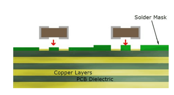
Figure 8 . Solder Mask3. Reduce size of Antipads
Antipads are where pads where copper is removed since this does not connect to any other plane. The smaller the anti-pad, results in clearer signal quality.
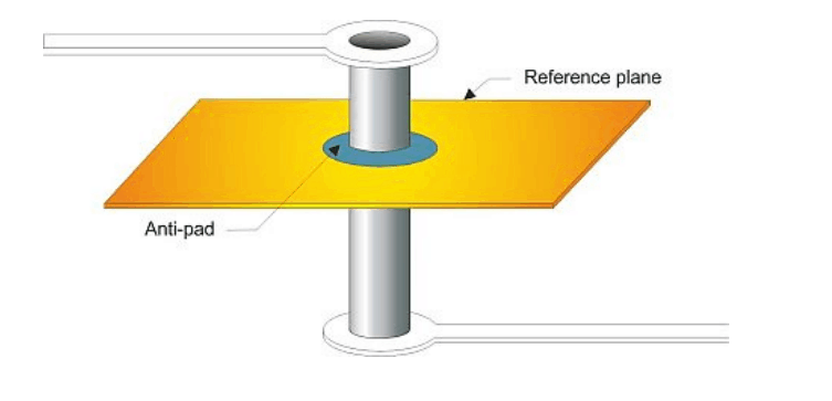
Figure 9. Antipads
- Avoid Much Pre-pegs
It is not a good practice to use more than 3 different types of pre-pegs in a stack up as this adds to total thickness. Prepeg should be below 10 mils in total.

Figure 10. Prepeg
MANUFACTURING CONTROLLED IMPEDANCE PCB
PCB manufacturer receives the design of copper, hole, and ink patterns, which are composed in a board with all the pattern sizes and positions within certain tolerances. In addition, the impedance from the trace is also determined with the tolerance of width, height, and dielectric thickness. Since there are limitations in achieving dimension requirements, the first pass is not as simple as targeting. When the first board is produced, adjustments are made to get as close to the target impedance as possible. A typical tolerance on final impedance is +/- 10%. As their process of manufacturing is composed of Etching, Engraving Photos, multilayer processing, and drilling masking, finishing and finally testing.
- PRACTICES OF MANUFACTURING
The following are practices of manufacturing PCB to achieve the desired impedance.
- Revised Physical Properties suggested by Manufacturer
It is usual practice that designs by engineers are reviewed by Manufacturers. In this manner, dimensions of track widths, copper layer spacing, copper weights, and the base materials are suggested for achieving the impedance required. Not only the manufacturers are knowledgeable in the tolerances produced from the manufacturing phase, but also has the access to industry standard software in impedance calculations
- Raw Material Inspection
Some Manufacturing companies have full strict on incoming inspection(IQC) for all laminates, pre-peg and copper foil. This is done since raw material thickness variances affect the controlled impedance of the circuit.
B. TOOLS USED FOR MANUFACTURING
The following are tools and equipment of manufacturing PCBs to achieve the desired impedance.
- Time Domain Reflectometry(TDR) Test
TDR testing is a method of ensuring correct impedance reading on a PCB upon producing. An electrical signal is sent to a PCB and is reflected back to the tester for extraction of the data. It is the measured impedance values over the distance of the PCB presented in graphical form. For ease of analysis, the data can be presented with average, standard deviation, minimum and maximum values.
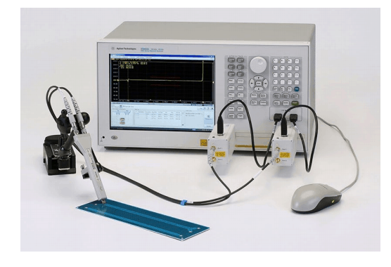
Figure 11. TDR
It is highly recommended for the analyzer to be reading an impedance capability of 150ohms with 1% tolerance. By this specs, a bandwidth of 7 gigahertz is attained supporting highly performing application PCB.
2. Laser Direct Imaging(LDI)
Laser direct Imaging equipment eliminates variances in trace width. Once the PCB has undergone this procedure, the configurations of the etching process and solution for the PCB has been determined to meet the desired impedance. This is also done to avoid under or over-etching.
Figure 12. LDICALCULATION METHOD
With the complexity and multifunctionality of today’s electronics board to meet the desired impedance, considerations are made to have verification methods to maximize signal integrity, minimizing noise, and eliminate reflections. The following common methods for determining impedance are made simple.
- SMITH CHART
The Smith chart is a graphical method to determine the reflection coefficient relationship between source and load impedances. It presents a circular plot with a number of interlaced circles to determine matching impedance. There are no computations required but it takes effort to read the parameters around the circle.
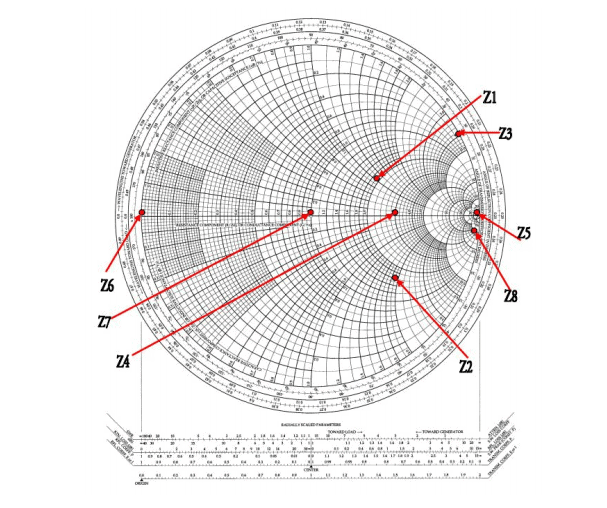
Figure 13. Smith Chart
In other words, the impedance matching is done by examining the load. And not only impedance is determined, but as well as other characteristics of the load such as admittance, gain, and transconductance.
B. COMPUTER SIMULATION
Control impedance calculation is mostly included in PCB design software that comes at expensive prices. One of its advantages is that other parameters are available for automatic modification for various simulations best suited for manufacturing. Popular software includes Altium, KiCAD, Eagle, EasyEDA.
- ONLINE CALCULATOR
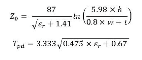
Every Impedance Calculator requires the same computing parameters namely substrate height, trace width, trace thickness in SI Units, and dielectric for both microstrip and stripline models. And also provide a guide in determining the best material suited for allowable dielectric constant. Every calculation is made from equations as presented below in case of Microstrip Impedance: Impedance calculating tools are available for ease of use online. Further parameters and details of different transmission lines presented below.
1. Microstrip
A microstrip is a transmission line with a flat conductor suspended over a ground plane. The conductor and ground plane are separated by a dielectric.
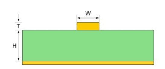
Figure 14. Microstrip
- Trace Thickness(T)
- Substrate Height(H)
- Trace Width(W)
- Substrate Dielectric(Er)
2.Embedded Microstrip
The embedded microstrip has a similar construction to the microstrip transmission line. A layer of dielectric material above the conductor is present and one case of an embedded microstrip transmission line is a microstrip trace with a solder mask.
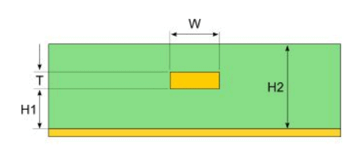
Figure 14. Embedded Microstrip
- Trace Thickness(T)
- Substrate Height(H1)
- Substrate Height(H2)
- Trace Width(W)
- Substrate Dielectric(Er)
3.Symmetric Stripline
The stripline uses transverse electromagnetic radiation. A stripline is constructed with a flat conductor suspended between two ground planes. Its advantage is its isolation between adjacent traces has improved.
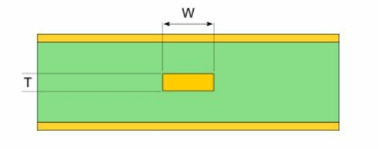
Figure 15. Symmetric Stripline
- Trace Thickness(T)
- Substrate Height(H)
- Trace Width(W)
- Substrate Dielectric(Er)
4.Edge Coupled Microstrip
The edge coupled differential microstrip is commonly used for routing differential traces. It is composed of two traces referenced to the same reference plane with dielectric material between them.
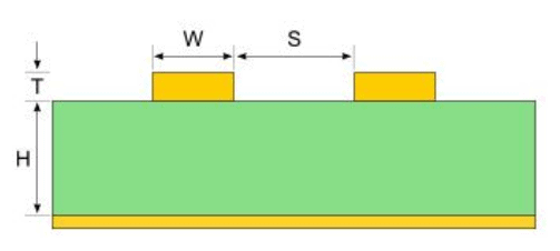
Figure 16. Edge Coupled Microstrip
- Trace Thickness(T)
- Substrate Height(H1)
- Trace Width(W)
- Trace Spacing(S)
- Substrate Dielectric(Er)
