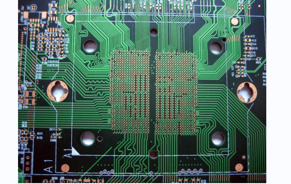
Any layer HDI PCB is the next technological advancement of HDI microvia PCB. The electrical connections between each layer comprise laser-drilled microvias. One primary advantage of this technology is that there is free interconnection between all the layers. Also, any layer HDI PCB integrates special technologies such as edge plating for ground connection and shielding, stacked vias, and minimum track width.
In addition, any layer HDI PCB integrates filled plating technology and laser technology. The use of laser technology in this board offers a high level of efficiency. This enables ultra-fine processing. Also, any layer HDI PCB has higher density wiring and higher degree of design freedom. Also, these circuit boards are suitable for downsizing smartphones and other electronic devices. Any layer HDI PCB offers layer interconnection and high density wiring.
What is HDI PCB?
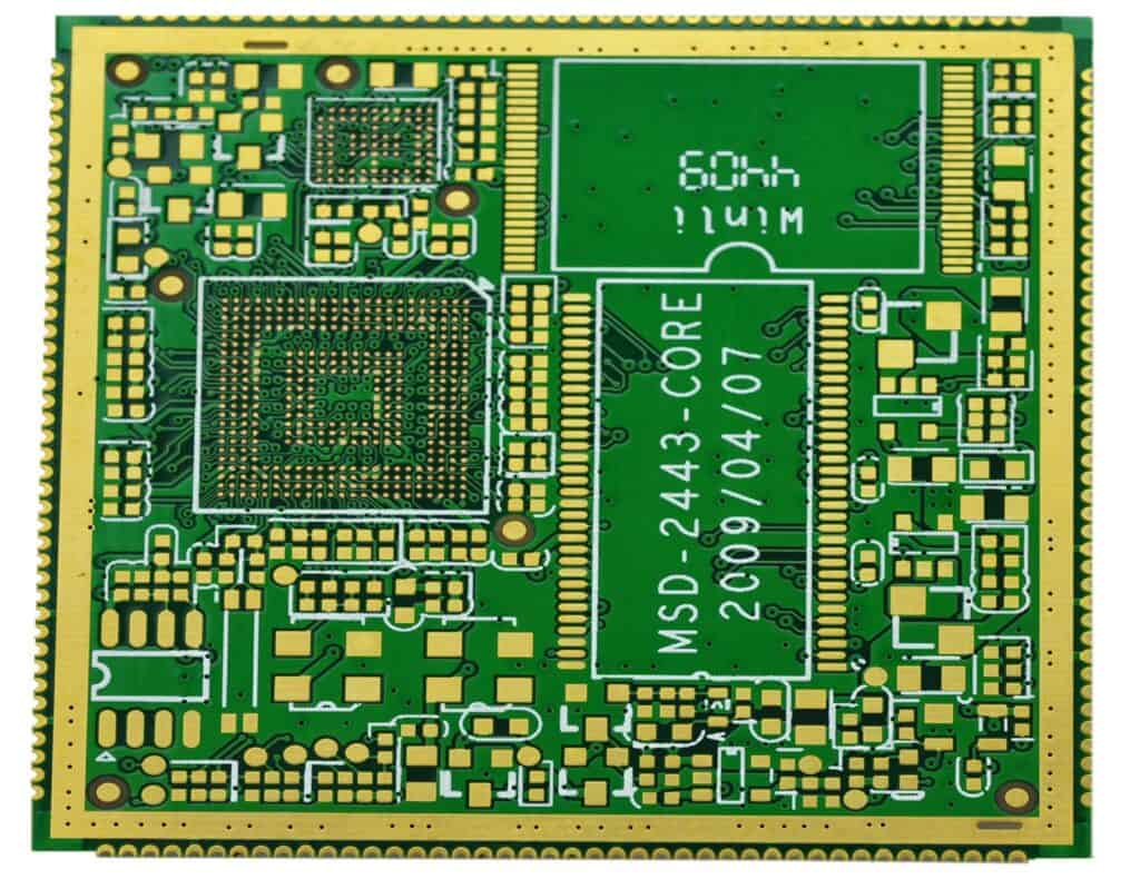
High density interconnect (HDI) PCB is a circuit board with more layer interconnections. The wiring density of per unit area of this PCB is more than that of a traditional circuit board. This means that HDI circuit boards have higher wiring density. Also, HDI PCBs have built-up laminations, buried and blind vias, and high signal performance.
HDI PCB technology has greatly contributed to miniaturization of electronic circuit and electronic devices. For more precision, an HDI PCB has an average of 160 pins for every square inch. Also, this design integrates versatile routing and dense component placement. The integration of blind vias, microvias, and buried vias helped in achieving a denser circuitry. HDI layer
Microvia technology gained more popularity in the PCB industry due to the advent of HDI. In an HDI PCB, there are more interconnections and these occupy minimal space. Also, the components in HDI PCB are closer. HDI circuit boards have much smaller vias, spaces, and copper traces. Due to their denser wiring, they are lighter and more compact.
Furthermore, HDI PCBs are multilayer boards that offer manufacturers the capability to achieve more with less. HDI printed circuit boards enable the integration of a large number of transistors. Therefore, this enables much better performance. Shorter distance connections also help in achieving signal integrity.
HDI circuit boards have the smallest holes and finest trace structures. Individual layers consist
Difference Between HDI PCB and Standard PCB
High density interconnect PCB offers enhanced signal integrity performance. This is because the inductances and capacitances of this board reduces due to the use of buried and blind vias. Also, HDI printed circuit board has no stubs. Therefore, the microvias’ impedance is very close to trace impedance.
Furthermore, a normal via has higher stray capacitance. This results in more discontinuity in impedance. HDI printed circuit board differ from standard PCB in various ways. For example, HDI PCBs integrate laser direct drilling while standard PCBs integrate mechanical drilling. Laser direct drilling offers more precision and accuracy than mechanical drilling.
Also, high density interconnect PCBs offer higher circuitry density for each square inch. The component density for standard through hole boards are less. In addition, HDI boards are usually more compact and lighter yet they offer more functionality. Standard boards are larger and heavier.
The HDI PCB technology integrates microvias, buried vias, and blind vias. Standard printed circuit boards integrate through holes. For HDI printed circuit board, there are less number of layers. However, standard PCB features more number of layers. HDI circuit boards are very compatible with low pitch packages and high pin count. On the other hand, standard through hole boards may not be compatible with low pitch packages.
Also, HDI printed circuit board is a cost-effective option. Since it doesn’t require more number of layers like standard PCB, this reduces the overall manufacturing cost. The layer interconnection in HDI printed circuit board helps to increase efficiency. Also, all the electrical connections on high density interconnect boards function well.
Furthermore, high density PCB offers more routing density and reliable interconnect solution than a standard PCB.
Lamination Process HDI Printed Circuit Board
High density interconnect PCBs are multilayer boards that comprise densely routed layers. Also, the lamination process holds the boards. Also, the high density interconnection layers are connected through the use of several types of vias.
The lamination process of a high density board begins with inner copper layer etching. After these, partially cured laminates separate the copper layers. Then the manufacturer stacks the layers with prepreg on bottom and top. After this, the manufacturer uses pressure and high temperature to press the stackup. The temperature must be high enough to liquefy the prepreg. HDI layer
After then, the liquefied prepregs becomes cool and bond the layers. The HDI printed circuit board will need to go through sequential laminations. The PCB will more expensive of there is more lamination. Designers can add more layers to enhance routing density. Also, sequential lamination helps to create complex designs.
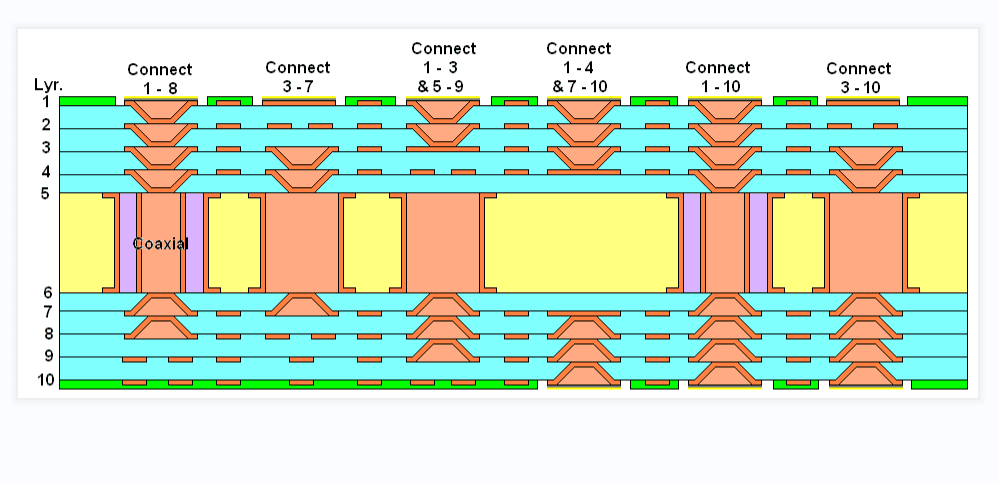
HDI printed circuit board can integrate several layering methods based on the requirements of the design. Here are common types of HDI stack-ups
1+N+1
This PCB stackup comprises 1 build-up of high-density interconnection layers. It is ideal for BGA having less I/o counts. Also, it is ideal for mobile devices like cell phones.
2+N+2
This is a complex HDI stackup with more than 1 build-up of high density interconnection layers. Also, it is ideal for BGA having higher I/O counts. This stackup offer better layer interconnection.
Any layer HDI
All layers here are high-density interconnection layers. Also, any layer HDI enables the interconnection of any conductors on HDI layer with copper filled stacked microvia.
Benefits of HDI Circuit Boards
These days, computers, televisions, and other devices are no longer heavy.
Also, these devices are compact and sleek. Electronic devices are part of human lives. They define how we live also. Modern electronic devices are now specially designed for compactness. HDI PCBs offer several advantages like:
Enhanced signal integrity
HDI boards integrate blidn-via and via-in-pad technology. Therefore, manufacturers can place components to each other. This helps to reduce the signal path length. Also, the HDI PCB technology gets rid of via stubs and as such, minimizes the reflection of signal. Hence, this helps to enhance signal quality.
Cost-effective
HDI printed circuit boards are a cost-effective option for advanced electronics. Also, HDI circuit boards offer more functionality than standard boards. For instance, a 6 layer HDI board offers more or the same functionality as a standard 8-layer PCB. The overall cost of manufacturing a HDI board minimizes since it requires lower number of layers.
Better reliability
HDI boards offer better reliability than traditional printed circuit boards. Also, microvias feature enhanced reliability due to their small aspect ratio. Furthermore, micorvias are more reliable than through holes as they offer HDI board with efficient performance.
Space saving
HDI board has more interconnections in very small areas. This helps to save space and as well contribute to the miniaturization of boards. Furthermore, the integration of microvias, buried vias, and blind vias reduces the board space requirement.
Faster time-to-market
Due to the design efficiencies of HDI PCB, it takes faster time to market. Also, the testing and design process for HDI PCB takes a shorter time. This is because it is easy to place components and vias.
Applications of HDI Circuit Boards
HDI PCBs are commonly found in complex devices that require high performance while saving space. The application areas of HDI PCB range from laptop computers, smartphones, medical devices, and military devices.
Medical devices
HDI PCB plays a crucial role in the health care sector. Also, most modern medical devices comprise HDI PCBs. Advanced medical devices like equipment for surgical procedures, imaging, and laboratory analysis. For instance, miniaturized cameras allow internal parts of the patients. These cameras are very small yet they offer high picture quality. HDI PCBs made it possible to produce such devices.
Wearable technology
Wearable devices like smartwatch, VR headsets feature HDI boards. Also, wearable technology is becoming popular among young folks these days. HDI printed circuit boards help to manufacture compact and complex devices. Also, you will find these boards in handheld and mobile devices.
Automotive industry
In automotive industry where less weight can enhance operation, HDI PCBs have proved to be very useful. Modern cars are becoming more computerized and connected. For instance, there are about 50 microprocessors in today’s cars. These microprocessors are useful in safety features, engine controls, and diagnostics. Several advanced features like backup sensors, onboard WiFi and GPS, and rearview cameras integrate HDI PCBs.
Military and aerospace
Military and aerospace devices are usually exposed to extreme environments. HDI circuit boards are ideal for use in these devices as they offer high performance even in hazardous conditions.
Industrial equipment
IoT devices are becoming very popular in warehousing, manufacturing and some other industrial settings. Most of these equipment integrate HDI technology. These days, businesses integrate electronic tools to monitor the performance of equipment and as well track inventory. Industrial machines comprise smart sensors that gather data and connect with other smart devices through the internet.
Conclusion
The benefits of HDI boards and any layer HDI PCB are numerous. With more interconnections, circuit boards can perform better. Also, HDI printed circuit boards contribute to the miniaturization of electronic devices used in several applications.
