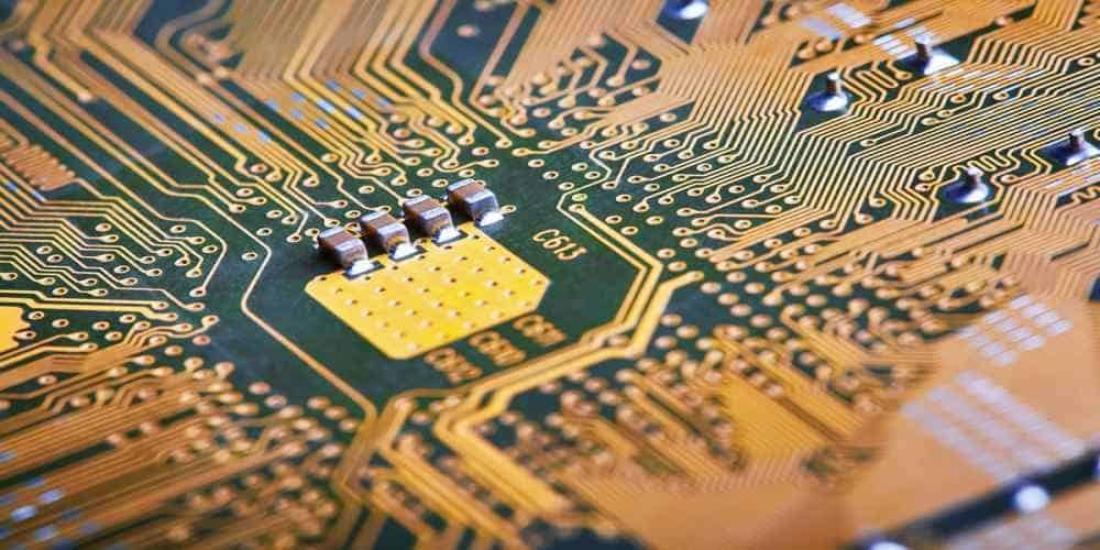
A high density board can make all the difference in your circuit board design. It is that type of Printed Circuit Board (PCB) that provides for the closer placement or positioning of the PCB components. This unification paves the way for the board’s signal integrity to be boosted, thanks to the dense wiring that also allows for faster connection on the board.
HDI PCB Definition
The main name for this type of PCB is the High Density Interconnect (HDI) PCB. It is so-called because of the higher densities that provide for better signal integrity, excellent wiring options and the realization of compact circuit boards.
The successful adoption and integration of the high density PCB design is not without the need for circuit boards to be smaller, and at the same time, paving the way for connections to pass with ease.
Thus, the density of the board has a lot of roles to play in the overall functionality. This is why we have lots of circuit boards high density PCB design to derive this benefit.
Identifying HDI PCBs the Easy Way
The integration of the high density interconnect process technology for PCB design is a great innovation, aimed at boosting the configuration of circuit boards for use with consumer electronics.
When it comes to the identification of such boards, certain pointers can help you place a hand on the HDI board with ease. One of such pointers is the usage or combination of different vias types for the design. The common ones are the buried vias and blind vias. The microvias is sometimes used.
It is expedient to mention that another way to identify the check the diameter of the vias used. Usually, this diameter is up to 0.006-inch or less.
The third way to identify the High Density Interconnect PCBs is by checking the number of pins used per square inch. If these pins range between 120 and 160, you can be sure that what you have is a HDI PCB.
The Effect of Interconnections in a HDI PCB
One major concern to the concept of high density PCB is the possibility of encountering some challenges during the design process.
However, this hurdle is effectively tackled with the help of versatile routing. This ensures that despite the strategic placement of the components, it is possible to still have these parts performing optimally, as the routing processes are versatile.
The versatile routing capabilities is connected to the HDI via-in-pad fill process. Also called the via-in-pad technology, it works with the microvias to help strengthen the signal path for the high density PCB. For this to work, the combination of the via-in-pad process (which is also a specialized copper plating process) with the microvias helps to densely pack the PCB components, while enabling versatile routing. This way, the integrity of the signals is maintained, while the speed of transmitting the signals is increased.
What Types of Vias are Required for High Density Boards?

Although we have made mention of the microvias, blind and buried vias, a lot more goes into the making of the HDI circuits.
In this section, we talk about the major vias processes that make up the high density circuit boards.
What are Vias?
Let us start by defining the understanding concept of vias. What do we call vias? To put it simpler, vias refers to the smaller conductive hole used for connecting multiple layers in a Printed Circuit Board (PCB).
In the case of the high density PCB, it is used for two purposes. The first is to connect the different layers that make up the board’s stackup. The second purpose is to facilitate the transmission of signals through the board – and at a higher speed.
Here is a breakdown of the different vias types used in the HDI PCB:
Buried Vias
As the name suggests, it is “buried,” hidden or out of sight. That aptly defines the buried vias – a type of vias placed or inserted into the inner parts of the HDI PCB. In addition to being hidden from the surface, the vias helps to connect two internal layers of a multilayered high density circuit board.
Blind Vias
While the terms “buried” and “blind” can be interpreted to mean the same thing in terms of not being seen, they are a bit different when used in the HDI PCB.
The function of the blind vias is to connect the internal layer and the external layer of a multilayered HDI PCB via a hole. The hole can be made with either laser or by drilling into the board.
Worthy of mentioning is that the blind vias is a bit strenuous to make when compared to the buried vias. Also, it is not entirely hidden. Unlike the buried vias that cannot be seen, the blind vias’ hole can be seen on one side of the PCB.
Through-Hole Vias
This type of vias follows the process of the Through-Hole Technology (THT). As with the THT process, it involves the lasering or drilling of the hole from the top to the bottom to enable the connection to the multilayered PCB’s layers.
If you are looking for a stress-free process of connecting the internal, external and all the other layers of a multilayered HDI PCB, it has to be with the through-hole vias. The versatility it brings is one major reason why it fits that description. Ideally, you have the options of choosing between the Non-Plated Through Holes (that don’t use copper pads) and the Plated Through Holes (that use copper pads).
Microvias
When a HDI Density Interconnect is said to be dense, it is mainly because of the use of the microvias. It is a type of vias that has the holes as the smallest, with at least 150 microns (or less) in diameter.
These holes, drilled with laser, are commonly used to connect one layer of the high density circuit board with the layer opposite it.
The benefits of choosing the microvias over the others (especially the through-hole vias), is the smaller diameter, which in turn, enables the design of denser PCB interconnect with complex designs.
Other HDI Design Attributes
Several features or attributes make up the workings of the High Density Interconnect (HDI). They include the ones we’ve talked about before – the buried, blind and microvias. It also includes the use of fine lines and spaces, and sequential lamination.
These features are designed with the aim of helping in the reduction of the size and bulk (weight) of the HDI PCB.
As for the sequential lamination process, it includes these two:
- Sequential Build-Up: this has to do with the sequential buildup of the layering process. The core consideration is to ensure the layering with at least two (2) press operations, especially for the multilayered PCBs like the high density circuits.
- Semi Sequential Build-Up: also called the SSBU sequential lamination process, it has to do with the pressing of the “testable substructures” in the Sequential Build-Up (SBU) technology.
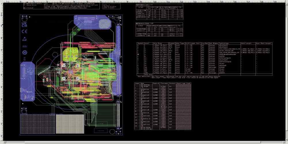
The Structures for the High Density PCBs
The structures, also called the HDI PCB stackup, refer to the overall presentation of the board’s layout.
Before we get into the different aspects of the structures, let us have a few points about the layout options for the PCB interconnect:
- These layouts refer to the techniques or processes used when map the physical output of the board. They are commonly used when the traces have their widths dropping below 0.2 millimeter.
- The compositions of the layouts include lower signal levels, thinner traces, higher layer counts and smaller vias.
With that being said, let us note a few points too about the HDI PCB stackup:
- The stackup for the board is made after the lamination process, which starts with the electrical interconnection of the densely routed layers.
- The HDI PCB stackup is pressed and heated to a point that it can liquify the prepreg.
- The stackup is considered completed when the liquified prepregs become cool and enable the sticking together of the layers.
These are some of the structures making up the High Density Interconnect (HDI) PCBs:
1. 1+N+1
This has to do with the use of blind vias, fine line and registration technologies capable of 0.4mm ball pitch to deliver a design stackup worthy of use with the Ball Grid Array (BGA) of lower Input and Output (I/O) counts.
2. 2+N+2
This is a type of HDI PCB stackup that use a combination of blind and buried staggered vias. Unlike the 1+N+1, which is the simplest to design, the 2+N+2 is a bit complex. The complexity includes the integration of two or more buildup of the High Density Interconnection (HDI) layers.
The attributes of the 2+N+2 HDI PCB stackup include:
- A thin finished board thickness
- Capable of being used with PCB designs that require a high-level signal transmission performance.
- Excellent interconnection of the conductors on the HDI PCB’s layer to the copper-filled stacked microvias structures.
- The capability to increase the routing density in complicated PCB designs.
The structures of the HDI PCBs also include 3+N+3 using the combination of blind and buried staggered vias and the 3+N+3 using blind/buried stacked vias.
HDI PCB Vs. Standard PCB
It is common to compare the performance of the High Density Interconnect (HDI) PCBs with those of the standard or traditional circuit boards.
The major difference between the two lies in the densities. The HDI PCB design packs more densities, even while maintaining the most compact of spaces on the circuit board.
The second difference is that the HDI PCBs, due to the densely-packed components and the minimal footprints, help to reduce the size and weight of the board. This often results in a smaller and lighter PCB – something most traditional circuit boards cannot boast of having.
The following are additional reasons why you should pick the High Density PCB connector over the standard circuit boards:
- HDI PCBs use less layers and have a limited aspect ratio.
- These circuit boards use a combination of laser and direct drilling, unlike the traditional PCBs that use mechanical drilling options, especially through-hole vias.
The HDI PCB Design Guidelines
It is important to talk about some of the processes or design guidelines that would potentially shape the outcome of the HDI PCB layout.
1. Use Fewer Layers
A couple of reasons suggest why fewer layers must be used with High Density PCBs. One such reason is the need to reduce costs. By using fewer layers, you don’t get to spend a lot of money buying more layers to be used for the design.
2. How Capable is Your Manufacturer?
One factor that influences the outcome of a HDI PCB manufacturing process is the manufacturer’s capabilities. As this is the major hand working on the board, you must be sure of the capabilities in that regard.
At Hillman Curtis, a top HDI PCB manufacturer in China, we have the requisite capabilities to make HDI PCBs, as per your requirements. You can also count on us for your all-in-one requirements, as we are a reliable Electronics Contract Manufacturing (ECM) company.
3. Don’t Leave out the Signal Integrity
One major benefit of working with an ultra high density PCB is to facilitate the signal transmission rate. As such, your HDI PCB layout should be designed with a streamlined set of design guidelines.
By scaling the signal transmissions, you can be sure that the board will fulfill the potentials.
Wrapping Up: Why Do We Use High Density PCBs?
If you are building electronics or consumer devices that require speed and excellent performance, using a High Density Interconnect (HDI) PCB to lay the foundation is important. The major advantage is the allowance for side-by-side placement of the components. This allows for the provision of enough space for more components to be placed on the board, while enabling the routing through the available spaces.
You can also use the high density PCB to improve the board’s thermal properties, via the use of laser drilling process to make smaller holes used for interconnecting the layers.
Some of the other reasons for choosing a High Density Interconnect (HDI) PCB are:
- Better signal quality
- Faster transmission of the signals
- Improved reliability and shielding from environmental conditions, thanks to the use of stacked vias.
- Finer track arrangement
- Higher wiring density
Now that you have chosen to work with the HDI PCB, it is important to choose an expert to handle the job. Hillman Curtis is an expert HDI PCB manufacturer that offers extensive coverage, and helps you place more components on both sides of the board, reduce the PCB’s size and save costs, compared to the conventional circuit boards.
