Printed Circuit Boards, or PCBs, are a significant factor to consider when discussing electronics. Whether talking about tiny gadgets such as smartphones and smartwatches or relatively large devices such as televisions, the term PCB will almost always pop up. That is because most of the electronics you will find today contain a PCB as a crucial component.
The primary function of a PCB on an electronic gadget is to route electrical signals through the device. By doing so, a PCB satisfies the mechanical and electrical circuit requirements. Simply put, Printed Circuit Boards direct electricity, bringing life to your gadget.
To carry out the electric signal routing, however, PCBs utilize a complex copper pathway network. The copper pathways deliver electricity to the various components that connect to the PCB. Moreover, the paths also determine the role of every element on the PCB.
However, though PCBs are pretty crucial to many electronic gadgets, their manufacturing procedure is not an easy feat. So how do manufacturers carry out PCB production? And what are the bumps that they come across while undertaking this task?
Before the Manufacturing Process
Before moving on to the Printed Circuit Board design, the circuit board designers need to take a brief tour inside a Personal Computer Shop. During the tour, they should ask the fabricators about their Printed Circuit Board manufacturing demands. By not skipping this step, PCB designers avoid making unnecessary errors that might lead to the failure of their project during the designing phase. However, since most companies are now outsourcing their Printed Circuit Board Manufacturing questions to suppliers from overseas, gaining this information has become a hassle.
Printed Circuit Board Production Process, stepwise
The Printed Circuit Board Design Process
Modern circuit Boards need to be pretty compatible with various printed circuit board layouts that designers develop using circuit board designing software. The most famous circuit board designing software programs that designer use include the following:
Moreover, to assist prevent issues emanating from inconsistencies, designers must advise their contract manufacturers before the PCB creation about the software version they used to make the circuit. Skipping this step might bring a lot of issues in the later stages.
Upon getting a reply, designers transfer the circuit design to a version the manufacturer supports. To share their designs with the manufacturer, PCB designers utilize Extended Gerber files. These are file formats that harbor PCB designs plus the various component that make the PCB manufacturing process smooth. Gerber files also go by the name IX274X.
Gerber Files in a Nutshell
Manufacturers utilize Gerber Files as the ideal or preferred output format for PCB designs. Moreover, these files bear critical information such as:
- Copper tracking layers
- Drill drawings
- Component notations
- Apertures et cetera
Gerber file-generation methods depend upon the Printed Circuit Board design program the designer will utilize. The more sophisticated the software is, the more options you will get to make your design more complex.
To ensure the circuit design is pitch-perfect, the designer must check every aspect of the Gerber file before submission. Moreover, to avoid flaws, designers primarily run an oversights algorithm on the PCB design. Furthermore, when evaluating the design, designers should also put into consideration such features like:
- Size of the hole
- Width of the track
- Hole spacing
- The board’s edge spacing
After carefully reviewing the design, designers send the PCB file to the Printed Circuit Board house, where fabrication takes place.
After receiving the PCB design, nearly all Printed Circuit Board Fabrication houses run DFM checks on them to guarantee:
– Minimal tolerance throughout the production process
– And compliance with the set standards
File to Film
Before the PCB Printing phase commences, designers must generate a Printed Circuit Board Schematic file. Manufacturers then carry out a DFM check on the schematic to approve the schematic for production.
Later on, manufacturers utilize a plotter that create the circuit board’s photo film. The manufacturer then uses the film to develop an image of the printed Circuit Board. You should also note that a plotter is not the usual laser jet printer, although it utilizes laser technology to carry out printing tasks.
Moreover, plotters utilize accurate printing technology, which helps them provide highly detailed PCB design films. These design films play a significant part in producing a PCB as they direct the manufacturers during the production process.
After the plotting is complete, the final item (the output) is a thin plastic sheet that the plotter prints using black ink. The sheet contains the PCB’s photo negative.
For the Printed Circuit Boards’ inner layers, black ink on the image represents the circuit board’s conductive Cu (copper) components. On the other hand, the portions of the non-conductive components are exhibited by the clear remaining part of the picture.
Moreover, for the outer layer, the images use reverse pattern:
– There is the transparent aspect for copper
– Black for portions that will undergo etching
After developing the film, the plotter then stores it automatically to avoid people tampering with the film before production.
Moreover, technicians must align a couple of films during production to achieve multilayers. To help ease this process, technicians at the film production stage need to punch holes in the films. The holes need perfect alignment; therefore, technicians take extra care during this process.
Achieving Perfect Alignment

To achieve perfect alignment, technicians must adjust the location, in this case, the table at which the films are positioned. They carry out regular adjustments until the table’s calibrations bring out a perfect match. After achieving the perfect match, they can punch the holes in the films.
The film’s holes fit into registration pins, and the manufacturer utilizes them in the imaging phase.
Inner Layer Printing
The generation of the film in the previous stage aims to bring out a clear “map” that defines the copper pathway of the circuit board. For the next step, manufacturers must print all the pathways on the film onto a foil of copper.
The inner layer printing stage in the PCB production process prepares manufacturers to generate the actual PCB.
Most circuit boards comprise a firm laminate board which has the following core components:
– Glass fiber
– Epoxy resin
Moreover, when technicians combine these two components, they refer to them as substrate components.
The laminates that technicians utilize at this stage are pretty efficient in terms of receiving the Cu that technicians use to structure the circuit board. Moreover, the two substrate components provide manufacturers with a dust-resistant and sturdy commencing point.
Inner Layer Processing
During inner layer printing, technicians pre-bond copper on both faces of the laminate. They then whittle away bits of the copper until they reveal the complex design of the pre-made film.
You should note that manufacturers do not care much about cleanliness during circuit board production. Therefore, they simply pass the output onto a decontamination chamber after whittling off the excess copper.
In the Decontamination Chamber
While in this stage, the technician must ensure that the laminate does not get dust particles. That is because even a small dust particle can render a circuit board useless due to short circuits and other functional problems.
After the Decontamination Chamber
When technicians finish removing all the contaminants in the PCB laminate, they now have to apply a photoresist onto the laminate. A photoresist is simply a photo-sensitive film layer containing photoreactive chemicals.
After direct exposure to UV light, these photoreactive chemicals harden instantly, which makes them perfect for the next stage.
When technicians prepare the PCB, they remove any chemical that hasn’t yet solidified through washing it using alkaline solutions. Moreover, technicians utilize a pressure washer for the final wash to remove anything that is not supposed to be on the board. Next, technicians need to dry the board.
When this production stage is complete, there should be resist adequately covering copper parts.
It is at this stage that a technician then checks the PCB to ensure no errors are present. Moreover, you should note that the copper on the printed circuit board at this point will remain on the board till the end of production. Therefore this stage is pretty crucial.
Moreover, only circuit boards containing a minimum of two layers must undertake this stage. Therefore, simple PCBs having two (or fewer) layers can skip ahead to the drilling stage. However, multi layer boards need to go through multiple steps.
Etching out Excess Copper
With the chemicals (photoresist) out of the way, and the now hard resist covering all the copper parts we need to keep, we can move on to the next stage: removing excess copper.
Just like how technicians use an alkaline chemical to carry out resist removal, they also utilize a chemical to etch away any unwanted copper particles on the board. However, technicians use a stronger chemical in this stage since copper tends to be trickier to handle when you compare it to resist.
To remove the copper particles, manufacturers have to bathe the board using a Cu solvent solution. The solvent solution removes the excess copper particles, leaving the copper pathways untouched.
You should also note that copper boards tend to vary significantly from each other. Some boards, mostly heavier ones, need longer exposure times and require higher concentration Cu solvents. On the other hand, some boards require less exposure time and less concentrated solvents. Therefore, manufacturers must focus on tracking spacing when working with heavier boards.
After removing the unwanted copper particles, technicians now need to wash off the hard resist shielding the copper pathways.
Washing the Hard Resist
To wash off the hard resist on the copper traces, technicians need to utilize another chemical solvent. The solvent removes the hard resist, leaving the board glistening with only the necessary copper substrates.
Optical Inspection and Layer Alignment
Now that the layers are clean, they will need alignment punches to ensure that all PCB layers line up perfectly.
To align the PCB’s inner layer with the outer layer, technicians utilize the premade registration holes. They then place all the layers inside a machine that they call an optical punch. The optical punch machine permits exact correspondence of the registration holes, which helps technicians align the layer accurately.
Once the layers are brought together, technicians cannot rectify any errors that might emerge from the inner PCB layers. Therefore, aligning these layers is of at most importance.
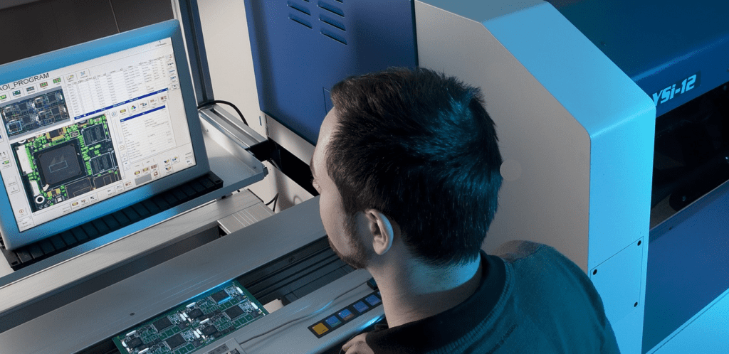
When this stage is complete, technicians utilize another machine to perform the auto-optical inspection. The auto-optical inspection machine confirms that the PCB is functioning correctly and it throws an alert whenever it detects an error. Moreover, the machine utilizes the designer Gerber file to check for defects in the design.
If the optical inspection machine doesn’t throw any errors, technicians can then proceed to the next stage.
Bond and Layering-up
In this phase, the printed circuit board now begins to take shape. Technicians now have all the PCB layers, and all that is remaining is to merge them, which will generate a single circuit board. For this merger to occur, the outer PCB layers must combine with the board’s substrate.
The bonding process occurs in two distinct stages:
– The layering-up
– The bonding
Layering up and Copper Foil Placement
The board’s outer layer component consists of the following:
– Epoxy resin
– Fiberglass
The epoxy resin pre-impregnates the fiberglass enhancing its durability and efficiency. Moreover, technicians also cover the bottom and the top parts of the substrate that holds the board’s copper tracing using copper foil.
When this process is complete, technicians can then sandwich the layers together.
Bonding
The bonding process happens on a steel table that contains metal clamps. Technicians place the layers on the table and secure them using the pins on the table. The entire setup needs to be pretty firm to avoid any inaccuracies from occurring.
Technicians then begin bonding by placing Prepreg layers over the alignment basins. The board’s substrate layer then fits over the board’s prepreg before the technician places a copper sheet onto it.
Moreover, the technicians place more prepreg sheets on the top part of the board’s copper layer. And to complete the stack, they then place copper press plates and an Al (aluminum) foil onto it. Now the layers are ready for pressing.
For pressing to take place, manufacturers utilize a bonding press program and a machine to carry out autoroute runs. First, the computer program instructs the device to heat the layers stack until they reach the temperature necessary for pressing. After achieving optimal temperature, the program then instructs the machine to press the stack, which binds the layers together.
After binding is complete, the technicians must manually eject the PCB from the machine for the next step.
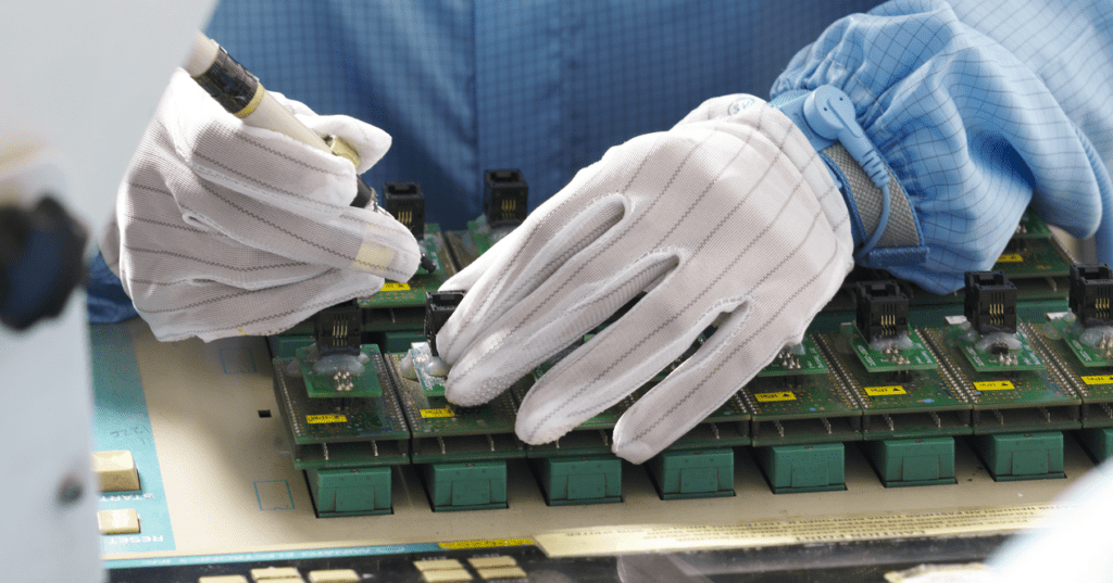
Drilling
For the drilling process, technicians utilize a computer-aided drill to achieve auto drilling. Using a computer to drill PCBs ensures accuracy and precision when drilling the various vias on the Printed Circuit Board.
For the actual drilling process, the computer-aided drill makes precise holes in the board, exposing interior panels and the board’s actual substrate.
After this stage is complete, technicians have to eject any leftover copper on the board.
Plating
After drilling, the PCB is ready for plating.
During the plating stage, technicians utilize a relatively strong chemical solution to fuse all the layers. They then clean the board thoroughly to remove any contaminants on the PCB.
Moreover, the chemical that technicians utilize to carry out plating seeps inside the vias on the PCB, creating a coating that protects the holes from external contamination.
Imaging the Outer Layer
For outer layer imaging to occur, technicians need to coat the outer layer of the PCB using a photoresist. The photoresist helps shield the PCB from UV light during this process. Hence it is pretty crucial.
During the actual imaging, technicians pass UV light on the board, which instantly hardens the resist.
Afterward, the technicians remove any excess photoresist and move on to the next stage.
Plating
Just like earlier, technicians plate the PCB using a pretty thin layer of Cu (copper). However, in this stage, they also apply another layer of a tin guard on the PCB. The tin layer, in this case, exists to shield the outer layer Cu from etching during the next phase.
Etching
To carry out etching, technicians utilize a chemical solution similar to the one used to remove exposed copper particles earlier on to eject any excess copper particles under the board’s resist layer.
After accomplishing this step, the technicians now have a PCB that has connections.
Applying Solder Mask
For solder mask application to take place, technicians must first clean the circuit board thoroughly. Doing so will eliminate the possibility of their being contaminants on the PCB from the previous steps.
After cleaning the PCB panels, the technicians must apply epoxy with a solder mask film. Immediately after applying the solder mask, the board turns green since this is the primary color of the solder mask.
To complete the solder mask application process, technicians must pass the Printed Circuit Board through UV light again. The UV light strikes and eliminates any excess solder mask leaving you with a clean Printed Circuit Board.
Silk Screening
The silkscreening process is pretty crucial since technicians utilize the silkscreen layer to apply vital information about the PCB, for example:
– The board’s serial number
– The board’s manufacturing company, et cetera
After silkscreening, the Printed Circuit Board has to undergo another coating and curing procedure.
Surface Finish
For this step, technicians plate their Circuit Boards using a finish that is solderable. The solderable finish increases the bond/quality of the board’s solder, which makes the PCB more efficient.
Testing
Before technicians consider a PCB a complete product, they must conduct electrical tests. Undertaking these tests helps the technicians confirm the PCB is functioning according to the blueprint’s design. Moreover, it helps them catch flaws in the PCB before delivering it to the client.
However, catching an error in this stage can be pretty costly to fix.
Factors that Affect the Amount of Money that goes into the PCB Manufacturing Process
Out of the many factors you should consider when constructing your PCB, only three will mainly affect the amount of money going into the project. These factors are:
– The materials that you choose
– The Printed Circuit Board’s size
– The number of PCB layers on your board
The Materials that you choose
The materials you decide to utilize on your PCB will affect the board’s cost of production immensely. If you choose high-quality components, expect the production cost to increase. However, if you decide to work with low-quality products, then the cost of production will be low.
However, sometimes you will have to go with high-quality products depending on how you wish to utilize your board. For example, if you use your PCB to carry out strenuous tasks under harsh environments, you will have to use high-quality products.
Printed Circuit Boards Size
The panel and the actual size of your Printed Circuit Board will affect the board’s production cost. However, the board’s size corresponds with the number of electrical circuits you will have on your Printed Circuit Board.
The most common dimensions that manufacturers work with are:
– 18 x 24 inches
– 18 x 21 inches
– 21 x 24 inches
Therefore, if your PCB exceeds these limits, you should prepare to pay more.
Number of PCB Layers
Typically, circuit boards with more than three-layer layers will require more effort to produce when you compare them with PCBs with two or fewer layers. Therefore, these circuit boards are pretty expensive to produce. Thus, if you want to build a budget-friendly PCB, then you should avoid a thick PCB.
Other Factors that also Affect a PCB’s cost of production include:
– Size of vias
– Minimum space and Trace
– The board’s aspect ratio
Conclusion
Printed circuit boards are, without a doubt, complex components that require much attention to manufacture correctly. Moreover, the production process tends to be stepwise, which makes it even trickier to achieve. However, using the directives in this article, you can develop your PCB while simultaneously avoiding unnecessary errors during the manufacturing process. Moreover, you can also budget for your PCB, which will help you generate a budget-friendly Printed Circuit Board.
