In modern technology, not only traditional lighting is in the market to compete with multiple applications. The demand rises for a more affordable and long lasting lighting object without compromising efficiency and expected output lumen. This gives advantage to LEDs to be introduced to households, outdoors,automotives and other industries.
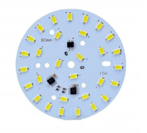
Figure 1. LED PCB
Innovations occurred when LEDs are soldered and mounted directly to PCB’s circuitry and now called as LED PCBA ( LED PCB Assembly ). It has different types in terms of materials and number of layers that come in multiple processes to be maximized to different applications.
1.LED PCB Design
There are multiple considerations in designing PCB, but the most important one is its corresponding cost without compromising quality. It is not as easy as randomly pl2acing LED components on board as both considerations are a must. In determining whether LED PCBs are optimized when it has good performance in thermal capabilities and capacitive coupling. That’s the time when the designed electronic product such as LED PCBs is manufacturable.
Another major consideration in the design process is its number of layers. It is composed mainly of Single, Double-Sided, and Multi-Layer PCBs. It is essential to determine the most suitable one for different applications. A simpler electronic device would benefit from a Single Layer while the more the design gets complicated, a more Multiple Layered PCB is necessary. And each of them differs in functionality and construction.
- Single Layer LED PCB Single Layer PCB Structure
Single-layer boards consist of one side where components are placed and a conductor on the opposite side, usually a copper. It consists of single substrate copper, a conductive metal layer, and then a protective solder mask with silk-screen. With the simplest structure, it is also the simplest layer of PCB to be considered in designs.
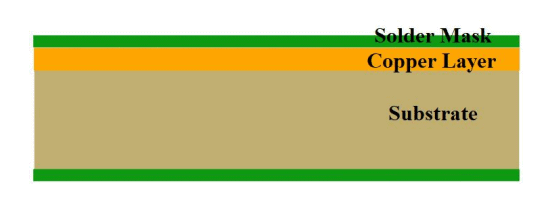
Figure 2. Single Layer led PCB
LED PCB Design Properties
A single layer PCB has limitations due to its size which can only accommodate components that can be fitted. And this limitation also brings an advantage such as flexibility.
- Flexibility
Every LED PCB has its copper as the thickest layer which is less than 1-ounce for a single Layer LED PCB. This is able to be flexed to fit any curve when attached to it when used as a strip. It can be folded and bent.
- Low-density Design
This layer type is best for the low-density design of electronic devices since there is only 1 side of the conductor. The lower the density means the lower the power consumption of the entire PCB.
- Operating Temperature
The normal operating temperature of a single-sided range between 130C to 230C. For an LED PCB, this design consideration is not a problem since LED produces less heat.
Advantages
This layer has the most advantage when used in producing PCBs in high volume with a simpler design. With its commonality, availability of resources, and ease of its production process, designing can be done with minimum issues; thus, resulting in minimal design and manufacturing costs.
Disadvantages
Having a single layer of the PCB means a limited number of components to be placed resulting in non-applicability to more power demanding electronic devices. With the limited space, only a few connections can be made which restricts the circuit to lower operating capacity.
Application
With its ease of production and low cost, this design is the most applicable to a part of a device responsible for a single function with no significant amount of data handling. This is usually found in common household and technology such as printing devices, LED, calculators, radios,and power supplies.
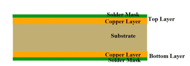
Figure 3. Double Layer Led PCB
- Two Layer LED PCB
Double Layer PCB Structure
Two Layer PCB has also one substrate layer but composed of 2 conductors with each side located on both sides of the PCB. This structure allows the design of having its component placed on both conductor sides. Through-Holes and Surface Mounts are methods applicable for placing the components on the PCB. Through-Hole is the traditional procedure where drilling the board is done and components are soldered through while Surface Mount is the method of soldering the components directly to the board.
LED PCB Design Properties
A Two-layer PCB offers more current, better heat dissipation and a more stable circuit in performing its duties. Below are its design considerations.
- Flexibility
Having 2 layers of copper in this type of PCB, it measures 2 ounces in thickness. Still, with this thickness, it has the ability to be attached to around the surfaces.
- More Dense Design
The added density to its property comes from the extra layer of conductor. A more dense PCB means more accommodation of LEDs.
C. Four Layer LED PCB
Four Layer LED Structure
Four Layer PCB is a combination of 2 Double Layer PCB. This is done by combining both PCB with a specialized adhesive. Since both contacting layers are conductors, insulation is done between them. And this design is considered for devices with a high number of connections.
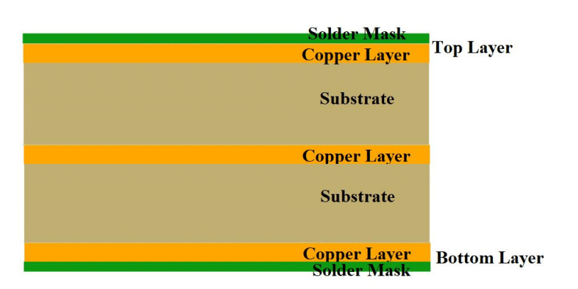
Figure 3. Four Layer PCB
LED PCB Design Properties
- Rigidity
This layer is best suited for producing solid hardware that retains in shape.
- Isolation of Noisy Nodes and Shortening of GND Path
With the available number of multiple layers, it can minimize Noise and shorten the GND path by following the design of components placement below. This is a common design consideration to maximize each layer.
- 1st Layer – Signals/ Power/GND
- 2nd Layer- GND
- 3rd Layer- Signal/GND
- 4th Layer- Signals/ Power/GND
This design is not only applicable to LED PCBs but also for other electronic devices.
Advantages
This type of layer offers its advantages to a more complicated design of PCB. It can handle a higher level of design complexity for a more significant added power, and speed. This is due to the added conductor allowing more components and connections to be accommodated. The more layers are added, the thicker product is produced; thus, making the device more durable to handle conditions. Despite its added components, it is still considered to be lighter than designing multiple single-sided PCB while maintaining the same functionality. And another property contributing to its weight optimization is its Single Connection Point which maximizes the connection between each component.
Disadvantages
With the complex design of a Multi-layer PCB, higher costs resulting from more resources, more time, and more skill occurs in designing, producing, and repairing. There is aswell a challenge in the availability of suppliers and manufacturers due to its complexity. With its disadvantages, the design has to be maximized by benefits outweighing the costs of producing multilayer than multiple single layers.
Application
With emerging technologies, the demand of complex circuits rises; thus, multilayer PCBs are utilized. This type of layer is maximized in the application of devices with huge data handlings such as different computer components, mobile devices, industrial machines and communication electronics.
2.LED PCB Choice of Material
- CEM
Composite epoxy material (CEM) is a type of material that is made from a cellulose-paper-based laminate having one layer of woven glass fabric. It composes of different types but what is mainly being used for LED PCBs is CEM-1. Other types are CEM-2, CEM-3, CEM-4, and CEM-5. They differ in properties and composition in handling flames and temperature. Each and every type has its advantages over the other but CEM-1 is the type that has the lowest cost and the most flame-retardant abling the material suitable for mass-producing LED PCBs.
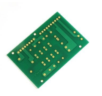
Figure 4. CEM LED PCB
CEM-1 being most applicable as a PCB material
Choosing Cem-1 offers low-cost production but is only limited to a widely used single-sided PCB application due to its impossibility of metallization through holes. With the rapid development of technology, single-sided PCBs are helping a huge amount of controlling other manufacturing and design expenses.
CEM-1 vs FR-4
FR-4 is the type of material also used for PCBs(to be discussed further later in the article). Both materials meet the UL94-V0 level flammability. FR-4 has the least vulnerabilities compared to CEM-1 in terms of physical properties making a lesser cost option in producing one-layer PCBs. Different criterion makes CEM-1 the most applicable basic material for producing LED lighting but the most important ones are its ability in achieving perfect balance between cost and heat dissipation without compromising performance.
B. Aluminum Led PCB
Aluminum is the type of material having single or multiple layers of copper with the metal substrate. It is used for applications of single and multilayer PCBs being able to accommodate applications of Power Converting Electronics. This also has the ability to direct away from the heat of any component making it applicable to LED PCBs design and production.
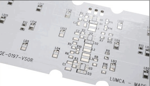
Figure 5. Aluminum LED PCB
By this property of the material in minimizing the harmful effect to other vital components, extending the useful life of LED devices is achievable.
Advantages of Aluminum PCB
Aluminum is one of the most thermally conductive materials that dissipate heat. Since it is physically durable, it is able to handle high-density circuits with multiple components with higher power demands. With its availability of supply, additional costs are not an impact. It is not only durable but also lightweight. It is dimensionally stable with only about 3.0% changes applied to its size when heated up to 150 °C.
Tradeoffs of Manufacturing Aluminum PCB
Aluminum is easily cheaper than copper but is sold more expensively without any components attached. This type of board has to be maximized by utilizing it in a more high-temperature application. It can be physically adjusted to be fit in a chassis but is unable to handle vibration. And Aluminum PCBs are mostly single-sided since producing double-sided PCBs are costly. There are multiple challenges in considering Aluminum as the material for manufacturing PCBs. One of which is the Etching process where the copper to be etched is thicker. Without proper controls in the manufacturing process, its width might be out of tolerance. Second is the Printing of Solder mask. Since copper foils are thick, it is difficult to print solder mask. And the third challenge is the Mechanical aspects of Manufacturing. Mechanical procedures involve milling and cutters which lessens the electrical strength of the material; therefore, the drilling parameters should prevent further deterioration of the material’s property.
Aluminum PCB Structures
Its structure is divided into four layers: Copper Foil, Dielectric, Aluminum, and Aluminum Base Membrane. Copper Foil Layer is the copper layer with its thickness relatively proportional to its current capacity. The Dielectric and Aluminum base layers are responsible for the material to be thermally conductive. And Aluminum Base Membrane is the layer that keeps it from unwanted etching and scraping.
- Metal Core
One challenge in the design considerations of the high-power LED is to eliminate its heat dissipation. With the advent of Metal Core material with its substrate able to effectively dissipate heat in its lighting, it paves its way to the market of PCB manufacturing. This material also has special magnetic conductivity, high mechanical strength, and special processing performance.
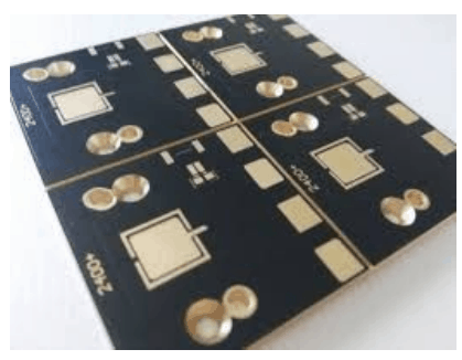
Figure 6. Metal Core LED PCB
MCPCB Structures
Metal Core PCB or MCPCB can be a single layer, double layer, or multilayer PCB. The simplest single sided MCPCB has a metal base that can be an aluminum or copper alloy. It is also composed of a Dielectric Layer. And same with common other structures, it has copper circuit and IC components with solder mask. A Double MCPCB consists of two layers of copper conductors. Basically, its composition is the same as the single-sided PCB with the metal core located in the middle to accommodate both conductors on top and bottom. And the multilayer MCPCB is just the combination of multiple single-sided MCPCB with the metalcore being in the center. Its components are the same and the more layers are designed, the more complex it is to be produced.
Advantages of MCPCB
If an electronic device accumulates a significant amount of heat, malfunctions occur. This can be prevented by using conductive cooling of transferring heat to a cooler part. This material possesses high thermal conductivity with thermal resistance able to conductively cool PCBs significantly fast. It is more lightweight than ceramics. They are non-toxic and are recyclable. And the most considered advantage is its high tolerance to vibration application due to its core that reduces its impact.
- Copper Base
Copper Based PCBs are the most expensive metal substrate with its heat conductivity property better than aluminum. It is capable of carrying a large amount of current by using a thick copper foil. It has a relatively small thermal resistance and its viscoelasticity is excellent, being able to withstand both thermal and mechanical stresses.
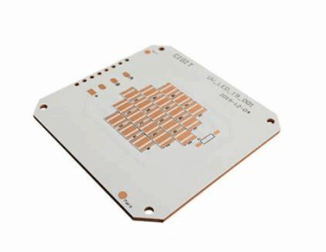
Figure 7. Copper Base LED PCB
Advantages of Copper Based PCB
Since the material is mainly made up of conductors, copper-based PCBs are low thermal resistant and high-pressure resistant. It is dimensionally stable withstanding mechanical stresses. It has good heat dissipation making it contribute to better grounding. And it has the ability to withstand thermal aging. Copper Based PCB has a wide range of applications, including Sophisticated Communication Equipment and Architectural decoration Industry. This is because that Copper Based is applicable to high-frequency circuit design and fields where sudden variations of temperature are necessary.
E. FR4 of led PCB
FR4 is another material that is being used in the production of PCB. It stands for ‘flame retardant’ and ‘4’ implies woven glass-reinforced epoxy resin. It has the property of mechanical strength and it is resistant to water being able to provide insulation for various electrical applications. This insulating property avoids signal interference; thus, promoting signal integrity.
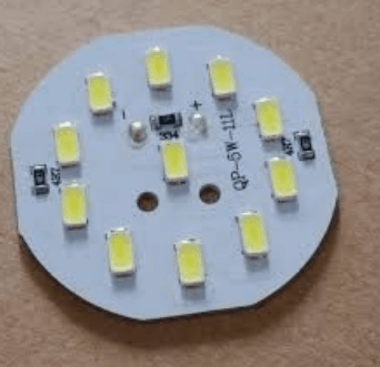
Figure 8. FR4 LED PCB
Challenges in designs of FR4 PCBs
Despite the complexity of FR4 material in PCB manufacturing and its property suitable to different applications, designers as well consider multiple limitations the material brings. One of which is its Soldering method that should be lead-free. This material is not able to maintain a constant impedance at high frequencies. It is also not applicable for the material to be exposed to high temperatures for longer durations making its applications limited.
3. LED PCB Manufacturing
- Material’s Heat Conduction
One challenge in design considerations of LED PCB is meeting demand for its expected lumen output while considering thermal conduction as more than half of the power consumed is turned into heat. Thus, this is needed to be removed from the circuitry to avoid damages to the components. This failure is called Catastrophic. And the more power is supplied to the circuit, the more it makes heat dissipation. One solution is to consider material of the PCB with low thermal conductivity.
FR-4
This is a commonly used PCB material with the property of flame retardant and has a very low thermal conductivity.
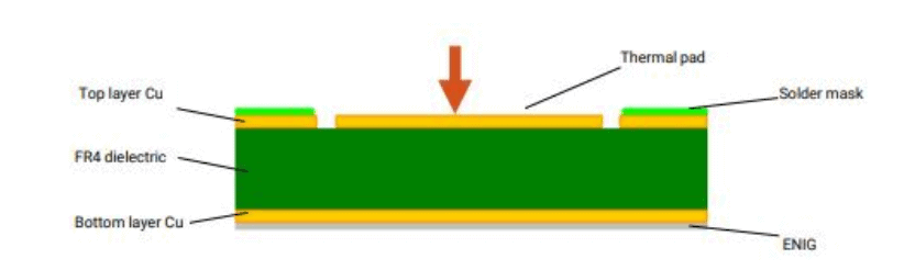
Figure 9. FR4 Conductivity
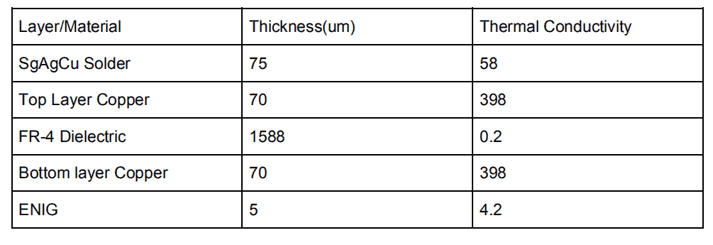
Table 1. FR4 ConductivityMetal Core
This material has a solder mask and different layers indicated below.
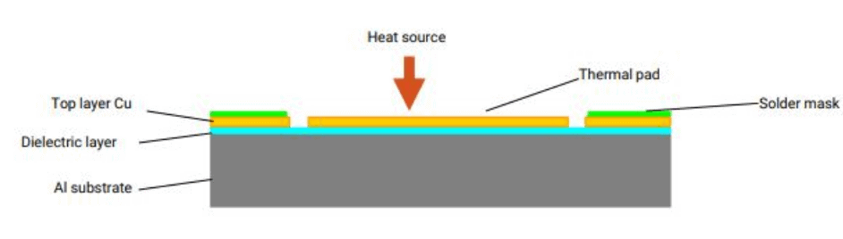
Figure 10. Metal Core Conductivity
Table 2. Metal Core ConductivityB. Solder Mask
One major consideration and parameter in LED PCB design is the color of Solder Mask. It is a polymer layer that protects the PCB from oxidation during the manufacturing stage. Sometimes its color represents personality while others consider it simply as a design. For the case of an LED PCB, matte black is mostly the option as it relatively associates LED’s resolution. Other colors may bring advantages and each of them are known for different applications.
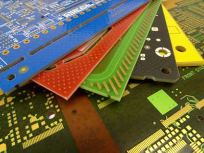
Figure 11. Solder Mask Colors
Color Application and Considerations
- Green
It is the common solder mask to be applied to PCB. This is because the components are clearly seen on this solder mask. When this is applied, the visibility of the traces between conductors are high. Since text is usually in white, this will produce brilliant contrast to enhance readability. As it is finished, reflection to lesser light is observed and glare is reduced. This is also applicable to white LEDs when applied to a PCB since both colors result in good contrast. It comes in a glossy and matte version depending on the brightness of the LED to be soldered.
- Red
This is the most professional looking solder mask among the other options. It has a property of good contrast on components and empty spaces. It is clean looking with a red solder used.
- Blue
When used with a mounted LCD panel, the finishes bring good contrast on edges, and bright background. This is often found on heavy boards. And it is considered as the most aesthetically good looking solder mask with components soldered.
- Black
As mentioned, it is best to use black for LED PCB because of its resolution. It is also unique in that it comes in both glossy and matte versions. It is often used for repairing processes. Its equivalent is white soler mask as its counterpart. It produces less contrast when labeled with slightly large electronic components. However, shadow is produced when light is absorbed. It is also being avoided when high heat is involved since it discolors the silkscreen.
- White
White solder masks are applied for clean looks in every environment. The circuit board will have a good contrast when lighting devices are attached to it in either matte or glossy version. However, white solder mask tends to hide traces as this makes inspection of PCB more difficult with limited lighting. But with black silkscreens, its appearance is highly recommended.
6. Yellow
As any other color, yellow presents a neat layout. It offers cleanliness, visibility, and style. With the available spaces between components and traces, it highlights its routing. However, this has not been common in standard as it appears to be poor in contrast with traces.
This implies it is the most expensive among the choices. It is usually used for submarine applications. This is one of the most expensive solder mask colors. A purple solder mask is basically used for submarine printed circuit boards. Application of the PCB is the major criteria in determining the solder mask’s color to be applied. It is a best practice to have samples of each color before proceeding to manufacturing.
C. Surface Finishing Process
A PCB surface is the finishing between electronic components and the board itself. When this is applied, there is the ease of soldering to properly distinguish copper layers. As there are various types, each offers different properties for several applications. But major criteria considers cost, reworkability, productivity, environment, and components to be soldered.
HASL and Lead-free HASL
This is considered as one of the most popular surfaces. But as time passed, limitations were realized. Since surface mounted components are trending, it does not provide reliability as it leaves uneven surfaces and not suitable for fine pitch components. In the manufacturing process, it has imperfections in being plated through-hole and poor wetting. For many cases, it offers availability, repairability and low cost.
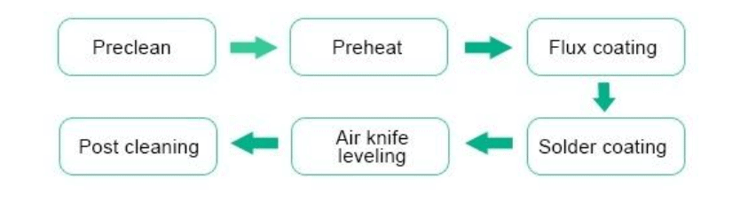
Figure 12. HALS LS HASL Process
- Preclean and Preheat
In most processes, this is to remove contaminants from the material in preserving the quality of PCB.
- Flux and Solder Coating
This process involves the PCB being sunk in a molten solder. This allows exposed copper in the layer to be covered with solder.
- Air Knife Leveling
In this procedure, it is necessary to eliminate extra solder from the preclean process. This is done by passing the PCB between hot air knives.
- Post Cleaning
In most processes, this is Deionization Rinse. It prevents building up of ions.
Organic Solderability Preservative(OSP)
OSP is the environmental friendly, water-based, and organic surface for PCBs. In the manufacturing process, the copper pads are protected to provide a coplanar surface. It also has the advantage of having a simple process, and repairability. But is sensitive and has shorter shelf life.
Figure 13. OSP Process
- Clean
This first process is to rinse off contaminants such as oil, finger prints, and oxidation film. Mostly these are organic. This is also to keep the surface bright and build the preservative in good quality. There is a standard in concentration of cleaning solution. This is kept to have standard OSP film.
- Topography Enhancement
In this process, it is where the bonding force between copper foil and OSP solution are improved. It uses micro etching to eliminate the oxidation from copper foil. This is also to have smooth and fairly even thick film; thus, maintaining a speed of 1.0 to 1.5μm per minute of micro etching should be done.
- Acid Rinse
Deionization Rinse should be maximized before building up of preservatives such as ions happens. This is when tarnish appears after reflow solder. And DI rinse also should be utilized after building up of preservatives with a maintained PH value of 4.0 to 7.0.
Immersion Tin (ISn) is the perfect design consideration for fine pitch and planar products. It works well for protecting the copper but it impacts its performance since the diffusion conflicts with their chemical property. It is cost effective and reliable. However, it is not good for PTH and tin whiskering.

Figure 14. Immersion Tin Process
- Clean/Micro etch
This first process is to rinse off contaminants such as oil, finger prints, and oxidation film.
- Micro dip
Before submerging to the Tin of the actual standard amount of tin, a partial dip is done.
- Immersion Tin
This is the main process of applying Tin to the PCB. It is done by submerging the material in an electroless chemical bath. This contains approximately 0.7 to 1.0 microns of tin to the copper.
- Postdip
In most processes, this is Deionization Rinse. It prevents building up of ions. This is also done to eliminate excess tin to avoid corrosion over time.
This moderate finishing surface is the most practically cost effective to be used for most applications for fine pitches. It lasts for roughly 12 months. It has the capability to prevent tarnishing and is stably high. But is sensitive to any contaminants in any form and friction. This has the same process as how to apply Tin finish but Silver is applied instead.
4. LED PCB Application
- Residential Lighting
By making the LED applications for Residents more affordable in the manufacturing process without compromising its quality, this gives way to LED PCB products to be introduced to the market of homeowners. It is more power-efficient and doesn’t contain mercury that harms an individual. It is as well diverse as offering multiple colors making a home more personalized depending on one’s preferences.
Efficient PCB LED lighting
LEDs are preferred in homes than the more traditional incandescent and compact fluorescent (CFL) due to its main advantages of being energy efficient and their capability to last longer. It is versatile in a way that it offers options for brightness and light appearance. It comes in a compact size with a number of shapes being manufactured giving homeowners different options in lighting multiple spaces of their house.
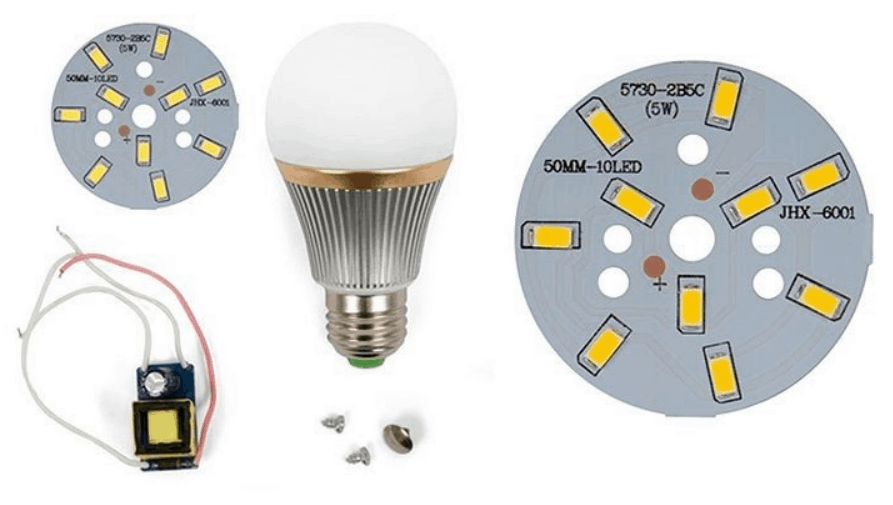
Figure 15. LED PCB Bulb
Smart Lighting Control System
One modern application of LED PCB is the automated Lighting System. It is a solution to using light more effectively and efficiently in a long term process by using a controller to automate its functions and thus enhances how the home looks. This system has several functions. One common of which is its ability to automatically eliminate or adjust lighting loads in any area. This contributes to power savings. And with the use of heat and light level sensors, the system responds to the environment to adjust the light levels accordingly. This system eliminates the old method of manual switching where all lights are switched on or off at the same time and by using rheostats for further additional control. There are functions that are pre-programmed features in this system that easily control the LEDs. This may include using selected LEDs at the desired light level or change colors of certain LEDs to enhance the look of the house.

Figure 16. Smart Lighting
Convenient and Portable Lighting
There are spaces in each home where cabling electricals for lighting are not conducive but proper vicinity is necessary. This could be under the sink for repair and maintenance purposes, kitchen cabinets for checking groceries or even checking spaces under the bed for lost items. This is where power-efficient battery-operated PCB LEDs are used. Some of them are remotely controlled while others use push-button for switching. With its convenience in easy installation and efficiency, it is one of the most suitable solutions.
B. Industrial Lighting
Industrial and commercial spaces should offer a productivity environment to employees and other workers within the vicinity. This is feasible by the choice of light. LED produces bright light to the surroundings that help in a clearer vision of the employees and avoids eye fatigue. It is also more comfortable and pleasing to the eye than the traditional bulb. LED offers color manipulation that conveys mood to the customers which are the desired setup of every commercial space in welcoming them. It is also practical to have LEDs in office and industrial places since they use less energy and can last longer. It produces insignificant heat that helps in managing temperature easier. In this manner, no further temperature control management is necessary.
Signage and Customized LED Displays
With the previous technology of fluorescent and neon lighting, LED paves its way to the market by bringing more energy saver and eco friendly LED lighting. This is used for directing business to storefronts with signage for marketing purposes.
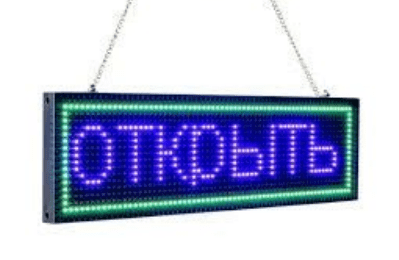
Figure 17. Industrial Signage
C. Automotive
In a wide range of applications of lighting, it is essential that mobile technology such as vehicles and other automotive advancements need efficiently low power in consumption to prolong battery life and have to be resistant to dust and moisture. This is where LED PCBs are much appreciated in the field of today’s Automotive Advancements where its different applications are presented below.
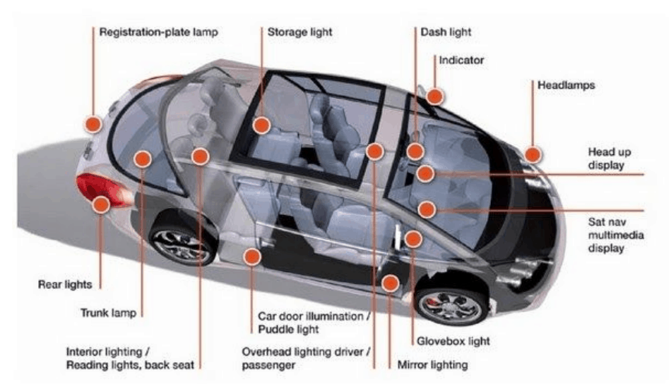
Figure 18. Automotive Indicators and LightingExterior Lighting System
Automotive Industry often uses Aluminum Based PCB LEDs in applications of Exterior LED Lighting Systems which composes of Headlight, Daytime Running Lamp, Taillights, Fog Lights, Door lights, Front Position Light, Side Marker Light, and other exterior lighting systems. With the property of Aluminum being durable and cheaper compared to other materials, it is highly recommended for Automotive Applications.
Interior Lighting System
LED PCBs are not limited to lighting and indications when automobile industries are observed. In its infotainment system where interior luxury design matters, Digital Display on Dashboards and Stereo Systems surrounding the car as well maximize the use of LED PCB which matches the essence and ambiance of how the car appears inside. The most complex in an Automotive System is the Powertrain. It is composed of the different modules controlling the behavior of the engine given the different sensors connected to it, namely, Mirror Sensor Accelerator Pedal Angular, Fuel Level, Motion Position, Steering Sensor, Throttle Position, and Transmission Sensors. There are multiple other sensors but these are the common ones. These provide indications on the Dashboard on an LED PCB.
Control Module Circuits
Engine circuits composed of Power Relays and Electronic Control Units where sustaining to high temperature is a criterion in maintaining its reliability, Metal Core LED PCBs are utilized. Since it has the property of withstanding to variations of temperatures, it is the material of choice.
D. Waterproof LED
Outdoor Decorations
Outdoor appearances are encouraged when there is some exterior lighting on landscape areas. Common practices of utilizing waterproof LEDs are adding light on Water Fountains, to illuminate Trees Bushes, driveway, post lights, and garage areas. These common areas are prone to temperature variations which Waterproof LEDs can withstand.
Solar Lighting
Solar clean energy powers independent PCB LEDs. These are commonly found on outdoor lawns, gardens, street lights. and even in remote areas where access to electricity is hardly found. By means of solar lighting, a conducive and eco-friendly solution is introduced.
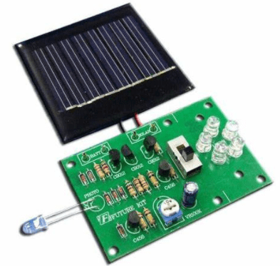
Figure 19. Solar LED PCBLighting
5. LED PCB Cost
Cost is the biggest factor of considerations when it comes to Manufacturing LED PCBs. It is not as easy as reducing cost to make less expense as the quality and deliverables have not to be compromised for several reasons. These are labor, technological advancements, packaging, and quantity. As most manufacturing businesses cover $10 to $50 varying to its quantity. Factors affecting additional costs cover in this section.
- Labor Costs
Labor costs depend on the geographical location of the manufacturers. Asia has countries with minimal labor costs. Even most manufacturing facilities have tools and machinery, labor is still required. In fact, what is really needed are skilled personnel with technical knowledge on PCBs. This is why labor costs significantly. Just to provide an image of how geographical location affects the cost is by comparing North America with $1100 quotation and China has its price of $550. This is with the same quantity.
- Turnaround Time
This is the factor that refers to the time span upto when the finished product can be done. Depending on the customer, the faster the deliverables, the higher the costs. It can reach upto additional 30% costs when deliverables are expected to be finished soon. In other words, this is the cost that the product is placed on priority including shipping.
- Quantity
What makes higher quantity lowers the costs, is the assembly costs due to economic scaling. Meaning, there is a significant drop in costs when higher larger quantities are considered. This is due to the fact that the initial costs are retained and maximized. And all units can be produced with no further initial cost. With this principle, higher volumes are best considered in making more profit.
- Parts Packaging
There is an exemption in additional labor cost when PCBs including LEDs to properly assemble and pack. Precautions should be observed in avoiding short-circuiting and malfunctionality.
6. LED PCB Manufacturer Criteria
Sufficient number of manufacturers are able to deliver quality LED PCBs for different applications consisting of computer, telecommunications, medical, automotive, aerospace, etc. this has to be done with good quality at a preferred competitive price. These are only a few criteria in choosing the right PCB manufacturing partner
- On Time Delivery
Every product has to be sold at a particular time frame. This is a critical job of most business owners to identify when a certain product can be sold easily. Even there are offsets and buffers in the quantity product, for most cases, this is negligible. This makes the delivery a factor for a company’s critical time that every delay is a loss of sales opportunity.
- PCB Design Support
Manufacturers are considered partners with customers. The company that designs requests manufacturers to produce the product; however, it is also a good practice that they provide feedback to customers in altering the designs to reduce cost while quality is not compromised.
- Advanced Manufacturing Facility
Every manufacturer should have the capability to produce any volume of products using advanced manufacturing equipment. This would gain trust of customers continuing business as these facilities ensure quality commitment.
- Customer Service
Manufacturing companies with excellent customer service respond to inquiries immediately by knowledgeable technical personnel.
- Ability to Meet Requirements
As any other contracts, the design specification should be met. This includes the right dimension, proper hole dimensions and positioning, proper soldering and right components to be soldered. In this case, the specifications of LED such as power rating and color have to be implied.
