Have you ever ordered for a Printed Circuit Board (PCB) only to have a different design and performance when it is delivered? Sometimes, the outcome of your board’s performance is directly proportional to the measures and processes used for the production.
Today, there are a wide range of testing processes in place to help make sure that the performance of the board is what you get at the end of the day. This is also why most PCB manufacturers have switched to using the In-Circuit Testing process.
In this article, we talk about one of the testing procedures called the bed of nails test fixture.
What is the Bed of Nails Test Fixture?
It is a traditional electronic text fixture used with the In-Circuit Testing (ICT) processes for validating the performance of circuit boards.
At the core of the PCB bed of nails performance is the detection and resolution of some of the defects and design errors associated with manufacturing Printed Circuit Boards (PCBs).
How the Bed of Nails Fixture Aids ICT
There are different kinds of testing procedures used to confirm if a PCB is functioning as it ought. Each of these processes are also optimized to check and facilitate the resolution of specific defects.
The In-Circuit Testing process or ICT, refers to the testing of the internal parts or components of the circuit board. As some of the design errors could come from inside the board, it makes sense to use the In-Circuit Testing (ICT) process to find and resolve them faster.
How Does the Bed of Nails PCB Test Work?
To understand how the testing process works, we will go back to look at the overview of the ICT process. For the In-Circuit Testing (ICT) to work, it has to use the bed of nails tester to gain access to the PCB’s nodes. This allows for the individualized analysis of each of the component’s performance.
The following explains how the bed of nails test fixture works when put to use in a Printed Circuit Board (PCB):
1. Composition
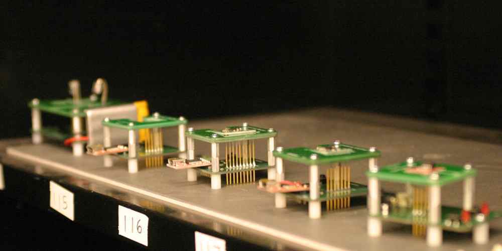
The bed of nails is so-called because of the composition of “nails” – which are the numerous pins that have been inserted into holes. These holes are hosted or hinged on a G-10 – an epoxy phenolic glass cloth laminated sheet.
Now, these holes are usually aligned with the aid of tooling pins, as a way of facilitating the contact-making with the test points on the PCB.
These holes are also connected, through wires, to the measuring unit.
2. The Contact-Making Process
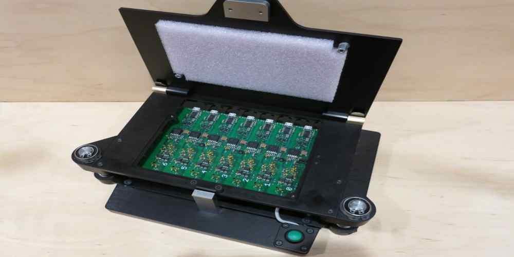
For the PCB bed of nails test fixture to make contacts with the internal components, nodes and test points of the PCB; they must be pressed down.
Due to the design as a set of small-sized, spring-loaded pogo pins, each of these pogo pins are enabled to make contacts with at least one of the nodes of the PCB.
Note: the contact-making has to be after the PCB has been marked as a DUT – device under test.
The DUT will now be pressed down as a way of having it pressed down against the bed of nails. This way, the different test points and other associated components in the DUT can be made to get into contact with the bed of nails.
The Scope of the PCB Bed of Nails Test Fixture
There are specific parts and test points that can be tested. Ideally, the testing fixture is used to check for both malfunctional or bad components, as well as overall manufacturing defects and design errors in the PCB.
For the PCB, the following are some of the critical focal points for the bed of nails fixture:
- It is used to make a single welding inspection.
- The bed of nails tester can also be used to check the components of the PCB that are “open.”
- It is also a veritable method of confirming if the circuit board is prone to short-circuiting.
How to Hold-Down the Device Under Test

The Printed Circuit Board (PCB)’s subjection to In-Circuit Testing through the bed of nails test fixture leads to its classification as a Device Under Test (DUT). That is, the PCB cannot be open to further development until the testing period is over.
The testing process works by holding down the DUT so that the test points can be penetrated by the pogo pins in the bed of nails. For this to work exceedingly, two methods can be used to hold-down the DUT.
Manual Process
This has to do with the use of your hand or asking someone to hold-down the DUT for you. Either way, the manual process can be hectic to carry out, will take a lot of time and the precision might not be that good.
This is often one of the major reasons why going for the mechanical process is better.
Mechanical Assembly Process
This refers to the use of mechanical assembly, mechanical process or a vacuum to hold-down the DUT to the bed of nails fixture for testing.
The mechanical process supports both the pressing down of the Device Under Test (DUT) from the top and the holding of the fixtures with a vacuum.
One of the benefits of using the vacuum process is that it gives a better reading of the signals than when the DUT is pressed down.
On the flipside, you might not want to rely on the vacuum process due to the following downsides:
- Non-Support for Automation: you will find it hard to use the vacuum fixtures when working with the bed of nails fixtures that have been designated for automated production lines.
- Cost Implications: besides, it will cost you a lot more to use the vacuum fixtures to detect internal issues in a PCB. The higher cost requirements are due to the higher manufacturing complexity associated with vacuum bed of nails fixtures.
Benefits of Using the Bed of Nails Test Fixture
You stand a lot of chances to detect errors and manufacturing defects in a PCB/DUT when using the bed of nails testing for a PCB.
Here are some good reasons why you should think in this direction:
1. Simultaneous Testing
Gone are the days when you have to wait in-line and spend a lot of money to have your PCBs tested. With the bed of nails test fixture, you spend little to gain more. The quick and simultaneous testing process is accentuated by the connection of the pogo pins to the hundreds of test points within the DUT’s circuitry.
This way, many test points and internal components of the DUT can be checked at once. At the same time, the prevailing issues and errors will be discovered in real-time.
2. Accuracy
From the different researches on bed of nails test fixture, one thing stands out – the fault location and detection is almost accurate. That way, you can trust or rely on the outcome of the tests.
Besides, these tests are carried out where they matter – the network points, specific PCB components/parts and device pins.
3. Reduced Maintenance Costs
Why allow an issue to escalate when you had a chance to nip it in the bud? Why allow an error or manufacturing defect in a PCB to crop up later than resolving the same now that you had the chance?
The importance of the PCB bed of nails fixture process here is to prevent you from spending a lot of money on maintaining the PCB when it begins to malfunction. By subjecting the DUT to the testing process, most of these defects and potential design errors are discovered and measures taken to address them on time.
Major Concerns Over the Bed of Nails Fixture Process
Despite the real-time and concentrated process of detecting issues in a PCB, the bed of nails test fixture might not be your go-to for circuit board testing.
Here are some of the peculiar downsides to it:
Potential Chances of Mechanical Failures
The risks of subjecting the Printed Circuit Board (PCB) to mechanical failures are there, especially if there are either high probe forces or poor support placement. Any of those two potentially triggers excessive circuit board flexure.
In return, the DUT/PCB is subjected or exposed to a wide range of mechanical failures, such as pad cratering, and capacitor flex cracking.
Production Volume
The bed of nails test fixture is commonly used for the PCBs with massive production. To this end, you may not be able to use it to make internal checks of the low-volume PCB productions.
Optimization Concerns
Optimizing or trying to rebalance the focus of the bed of nails fixture is an issue. It is so because of the inability to optimize or rebalance the fixture for both the probe forces and support locations.
Even if you were able to do that, it often comes with additional expenses expended towards the designing and building of an In-Circuit Testing (ICT) fixture.
Final Thoughts: How to Get the Most out of Bed of Nails Test Fixture
As an integral part of the ICT testing process for PCBs, the bed of nails PCB test helps to make a simultaneous detection and resolution of some PCB design-centric issues.
A careful observation of the test points and the fixing of the detected issues are some of the benefits you get from having your PCBs tested by Hillman Curtis.
