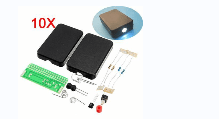
If you deal with electronics or are generally an electronics enthusiast, you will most probably come into contact with PCBs a lot. That is because PCBs have become a crucial element in the electronics industry. Using PCBs help manufacturer produce sleek, thin electronics with a lot of processing power. Moreover, these elements are lightweight, and hence they also reduce the weight of the resulting gadget. However, although PCBs are beneficial to the electronics industry, manufacturers have a hard time manufacturing them due to the complexity of the PCB manufacturing and assembly process. Due to this reason, they tend to charge a lot of money to produce PCBs, either in bulk or in single pieces. Moreover, the price goes even higher when you request a custom PCB.
But what if there was a way to produce your PCB at home without needing heavy-duty equipment? , All you require are some tools, for example, plastic tweezers, thinner, a tiny container, a miniature drill, and a small amount of ferric acid, plus some necessary materials for producing a PCB. Moreover, the DIY process is relatively simple, taking about 30 to 45 minutes to complete.
What is a DIY Circuit Board, and How Can I Build One?
A DIY circuit board is an electronic component assembled by a person. It is a common task for people who want to build their own electronic devices.
The first step in building your circuit board is to decide what you want to build. This is the most important decision you will make. Next, you design your circuit in your head and then draw it on paper. We recommend taking a picture of your project to see what it looks like when complete. Your circuits must be large enough to fit inside small areas (in our case: a bookcase).
Next, you must ensure that everything fits together properly and operates correctly before moving on to the next step: testing your circuit board. Testing involves checking to see if the circuit is working properly and that the circuit board needs to be replaced. If you’re unsure whether your board is broken or has been damaged during shipping or storage, visit your nearest electronics store for help. Remember that a malfunctioning circuit board can damage an electrician’s tools and equipment when he tries to remove it.
What exactly is a Printed Circuit Board?
PCBs electrically connect and mechanically support electronic components via pads, conductive tracks, and other elements etched from thin copper sheets. Moreover, the copper sheets are laminate on a substrate that is non-conductive which reduces the chances of short circuits.
Printed Circuits Boards bear pre-designed tracks of copper on a conductive sheet. By using these predefined copper tracks, manufacturers can reduce wiring; hence, they automatically reduce the weight and size of a gadget. Moreover, due to less utilization of wires on PCBs, manufacturers can reduce the number of faults that tend to arise because of loose connections. As a result, all technicians must do to connect various components to a circuit board is, place them onto the board and then solder them.
Different Variations of Generating a Printed Circuit Board
To generate functional and efficient PCBs, manufacturers utilize the following three methods:
- Laser cutting-edge etching
- Circuit by hand
- Iron on glossy paper
However, the first method (the laser method) tends to be the industrial technique manufacturers use to mass-produce PCBs. This method tends to be pretty expensive to undertake; hence, it is not very beneficial when producing a DIY PCB. However, the remaining two methods are easy to undertake, so you can efficiently utilize them to create your DIY PCB.
Stepwise Directions to help you DIY your Circuit Boards
Gather Materials and Tools
The first step in generating a DIY PCB is to find all the necessary materials and tools to undertake the project. The materials that you will require for the project are the following:
- Sanding paper
- Tiny cloth pieces
- Plastic straw or plastic tweezers
- Magazine papers or glossy paper
- Ruler (optional)
- Marker Pen (fine-tuned)
- PCB Board
- Etching Solution (preferably Ferric Chloride)
Once you have all these materials, you can then move on to gather all the necessary tools. The tools that you will require for these projects include:
- Latex gloves
- Laser printer or a photocopying machine
- Eye protection
- Flat iron
- Mini Drill or a Dremel
Once you have all the materials and tools required to produce your DIY PCB, you can move on to the next phase.
Developing your own Printed Circuit Board Design
If you already have a Printed Board Layout, you can move on to the next phase. Moreover, if you plan on writing your own PCB design directly onto the Circuit Board, instead of generating the circuit diagram file first, you can also move on to the next phase. However, if you want to develop your custom PCB design, this step will significantly help you. To do so, you can utilize the many printed Circuit Board Designing software in the market. These software programs include:
- PCBWizard
- Autodesk Eagle
These efficient open-source programs can help you convert your circuit’s schematic description to a Printed Layout that you can utilize for the production phase. Moreover, if you prefer to avoid the hassle of using complicated software programs, you can utilize Microsoft PowerPoint, which can do the same task efficiently.
Generate your Design Printout
When generating your printout design, stick to photocopying machines and laser printers. That is because a printout design from an inkjet printer tends to be inefficient for later production phases since the ink in use is soluble in water. Therefore, the Printout tends to cause issues when transferring the design to the bare board.
Moreover, you can utilize any magazine or glossy paper to undertake this step. However, to be specific, the following types of paper will produce better results:
- Glossy paper
- Magazine paper
- Photo paper
Points to remember when producing your Printout
During the printing process, it will help to keep the following point in mind:
- Pick the mirror Printout
- The output should be set to black for both the printer driver and Printed Circuit Board Design software
- Ensure to print your design on the paper’s glossy side; this will produce better results
Cut Copper Plate
For the next phase, you will have to cut a copper plate that will house your PCB design. The copper plate should correspond in size with the board’s layout.
You can utilize a cutter or a hacksaw to cut the copper plate.
After cutting the copper plate, you should then rub the PCB’s side that has copper using an abrasive sponge or steel wool. Doing so will remove the oxide layer on the top part of the plate, and it also gets rid of the photo-resist layer. Moreover, sanding helps the design image on the Printout stick more efficiently onto the board, producing a better image to use.
Transferring the Printed Circuit Board Printout
To transfer the design printout onto your copper plate, you can use one of these two methods:
Method one: Glossy Paper technique (Great for more complex circuits)
The Glossy paper technique involves taking the printout paper (bearing the board design) and transferring it into the copper plate. To achieve this feat, first, flip the top layer horizontally, then place the surface of the copper plate that has copper onto the printout paper. Next, ensure you align the PCB board correctly with the printout design to achieve better results. Once this is done, you can utilize a regular laundry ironing box to iron the printout paper on the PCB board.
Place the photo paper and copper plate set on a wooden table (it should be clean to reduce contaminants) with the photo paper’s back facing you. Then using a spatula or pliers, hold on to one end to keep the setup steady during the ironing procedure. Once this is done, place the ironing box, which is now hot, on the opposite end of the copper plate for about ten seconds. You can iron the printout paper via the ironing box’s tip while applying slight pressure when complete. Carry out this procedure for around five to fifteen minutes.
Doing so will efficiently transfer the ink on the paper onto the Copperplate. And since the ink placements correspond with the PCB layout design, you will have the entire design on the copper plate. However, as per temperature adjustments on the ironing box, you should utilize higher temperatures for thick papers and low temperatures for thin to medium papers.
After ironing Procedures
For this next phase, keep in mind that the copper plate is hot due to the ironing procedure. Therefore, you should refrain from holding it using your bare hands.
After ironing, you should place the copper plate, with the printout paper still intact, inside lukewarm water and let the setup stay there for around ten minutes. During these ten minutes, the printout paper dissolves efficiently, and you can now gently eject the paper from the board. For better results, avoid pulling out the paper hurriedly. Instead, peel it out of the board from a slight angle.
Sometimes, when ejecting the printout paper, you might note that some tracks become faint. If this happens, do not panic; you can use a marker pen to darken the spots efficiently.
Method two: By hand (Effective only for small and simple circuits)
To achieve the “by hand technique” of transferring the board design onto the copper plate, you will require a pencil and a fine-tuned marker pen. Then, using the pencil, you will have to manually sketch the design onto the board using the Printout as a reference. Once you complete the sketching process and are sure that the design is accurate, you can trace the sketch using the marker pen.
Sawing and Sanding the excess Copper Plate
Now that the design is imprinted efficiently on the copper surface, you can quickly tell whether the copper plate is big or small. If the copper plate is big, you can quickly reduce its size using a standard metal saw. Doing so will make the board more compact and hence more efficient. Once you saw the excess portions of the copper plate, you should smoothen the board’s edges by sanding them using sanding paper. Moreover, to gain a better finish, you can utilize a finer; this gives your board a better look and feel.
Cleaning and Restoring the Board
Even after dipping the board in the water and carefully removing the printout paper, chances are that there will still be some excess paper remaining on the copper layer. To remove these contaminants, you should utilize sharp objects, for example, a toothpick.
Moreover, after the sawing process, you probably unintentionally rubbed some ink off the copper plate. Therefore, you should restore these faded regions using the fine-tuned marker pen for better results in the next phase.
Etching the Printed Circuit Board
When carrying out this step, you must be extra careful as it involves using chemicals. Firstly, put on plastic or rubber gloves to shield your hands. Next, cover the bottom part of your etching setup (the container that will hold the etching solution) with newspaper to avoid spilling the etching solution on the floor or table. Then, fill the plastic container with water and dissolve around 2 to 3 teaspoons of ferric chloride. Next, dip your Printed Circuit Board inside the Ferric Chloride Etching solution for about 30 minutes.
During these 30 minutes, the FeCl3 (Ferric Chloride solution) will react with the bare copper (the copper that is not covered by ink) and ultimately remove all the excess copper from your copper plate.
When the thirty minutes are over, remove the PCB from the solution using pliers and check whether the excess copper has been removed efficiently. If any unwanted copper remains on the board, you can re-dip the board inside the FECL3 solution for longer or until you are satisfied with the etching process.
Disposing of the Etching Chemical Solution
While disposing of the etching chemical solution, you should be extra careful since the solution tends to be pretty toxic to sea creatures and plants. Refrain entirely from pouring the solution inside a tap after completing the etching solution; this is illegal, and doing so could get you in trouble. Moreover, pouring the solution into a sink might damage your pipes.
However, you should dilute the chemical solution using water and dispose of it safely.
Rinsing the PCB
After the etching process, you should rinse the PCB to remove contaminants. For this process, again, ensure you protect your hands using protective gloves. Moreover, it is important to use plastic tweezers to hold the PCB for extra protection. Avoid using metallic materials such as pliers to hold the PCB as the chemical solution will make the material rust within a short period.
Removing the Ink from the Board
You can use a regular toothbrush and laundry soap to remove the ink from your PCB. Brush the ink using laundry soap to expose the copper tracks left behind after the etching process.
However, if you do not have a toothbrush and laundry soap up close, you can still utilize sanding paper (preferably fine sanding paper) to clean the ink. Sanding paper is pretty efficient and gives the PCB a shiny finish.
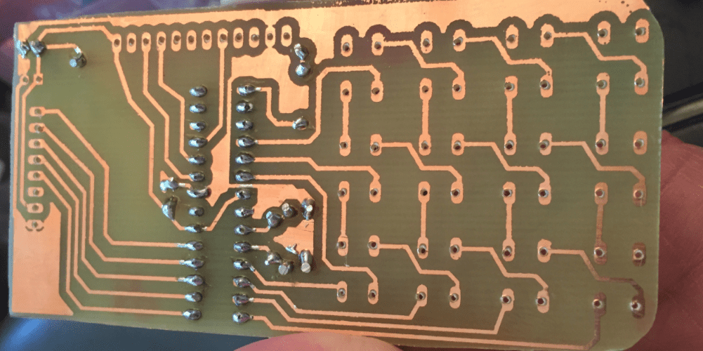
Drilling Holes
You should utilize a Dremel or a miniature drill to drill holes through the PCB. Using this drill, you can generate tiny and precise holes to connect various components to your Printed Circuit Board.
After the drilling process, rinse the PCB again using water. Moreover, ensure you drill on the side with copper because the copper tracks will guide you on where to place your VIAs.
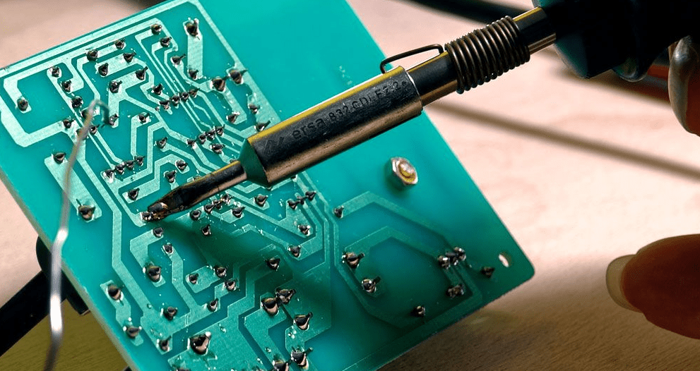
And that is it; you have your DIY PCB. Ensure you clean it again before you solder any components using a solder mask and a soldering iron.
Benefits of Generating a DIY PCB
Saves Time
Most people assume that generating custom PCB designs and building the board at home consumes more energy and time than contacting a manufacturer to generate the board for you. However, this assumption is wrong since developing your PCB design and producing your PCB via DIY saves you a lot of effort and time. That is because manufacturers tend to take their time in creating PCBs. Therefore you will have to wait for a while before you receive the PCB from your manufacturer.
However, you can complete production in a single day when you generate the board at home.
The designing phase is usually the most complex phase of production and takes a lot of time. However, using the right software program, you can quickly generate your PCB design.
Moreover, since DIY means that you are creating the PCB at home, you cut down on time you could have spent waiting to receive the shipment from your manufacturer. You can then utilize this extra hour to optimize your PCB or generate another one.
Reduced Labor Costs
When it comes to PCBs, the cost of production mostly goes up due to labor costs, not even material costs. Therefore, when you develop your Printed Circuit Board design, you save on the money that could have gone to a PCB designer. Moreover, when you produce your PCB via DIY means, you save on the money that could have gone to PCB fabricators and assemblers. Therefore, overall, by reducing labor costs, you save a lot of money.
Moreover, custom PCBs require fewer adjustments and re-work, where labor costs tend to pile up. Additionally, you can still utilize the schematics to generate a similar PCB if needed when you finish your initial PCB.
Flexibility
When generating a PCB via DIY means, you have more freedom and flexibility to fix and adjust elements along the production process. Therefore, rather than waiting for the entire assembly of the PCB to identify and rectify a bug. Instead, you can detect the bug early and then make necessary adjustments to fix the issue. Doing so will save you a lot of time and resources that could have gone into fixing the bug at a later stage.

Technical Control
Generating your own circuit boards via DIY means places you in technical control as far as the project is concerned. You dictate what is to happen next in the project. Hence the outcome is tailored to your desires.
However, this bears some drawbacks, such as revisions and problems falling on you. Therefore, if any errors occur in the production process, you tend to hassle alone to fix them before they escalate.
Disadvantages of a DIY Printed Circuit Board
Even though producing a PCB via DIY means has a lot of advantages, it also has some disadvantages, which include:
Voltage
One main issue you might face while developing a DIY PCB is assigning the board the wrong voltages. And since the main or the only purpose of a PCB is to transmit current, this error can mess up your board entirely. Moreover, having the wrong current flowing through the PCB can even cause drastic results after assembling components into the board. So to avoid these errors, ensure your assign accurate voltages to your design.
Poor Designs
When it comes to PCB production, the design of the circuit board matters a lot. That is because the printed layout dictates how the PCB will function. Unfortunately, DIY PCBs are prone to poor design, which sometimes might even render the PCB useless. Therefore, you should review your plan thoroughly to catch and fix any design errors before you move on to production.
Moreover, the schematics and documentation of the PCB have to correspond. Therefore, any discrepancies might confuse other people looking to utilize the PCB.
Post Production Assembly Errors
Sometimes, people tend to place components incorrectly during the assembly phase. Incorrect placement of components can cause drastic effects, especially when the PCB is connected to a power source.
To avoid such mistakes, connect each component to its corresponding VIA. Moreover, cross-check the components before connecting the PCB to a power source. Doing so will save you a lot of trouble.
Is it worth it to buy a DIY Circuit Board Maker?
We generally think of DIY circuit board makers as hobbyists and enthusiasts. However, they are not the only ones who can make a DIY circuit board. Many people can do it too. As long as you have the right tools, you will easily create your circuit boards.
Conclusion
Printed Circuit Boards are primary elements in the electronics industry. Therefore, technicians in this industry greatly utilize circuit boards in their projects. However, producing them via a manufacturer every time can be pretty costly. However, following this article’s instructions, you can quickly generate a custom PCB at home using simple tools and materials. Doing so will save you time and money. Moreover, you will get to customize your PCB to your exact needs; hence your imagination is your limit.
