Trace, in the context of PCBs, typically refers to the board’s network of insulation, wiring, copper, and fuses. If electronic equipment is malfunctioning in any way, the PCB tracing is almost certain to be inconsistent. And in the field of printed circuit boards, electronic engineers use the word “trace resistance” most frequently. Additionally, trace resistance refers to the components of a board that act as barriers to the free flow of electricity.
What is a Copper Trace PCB?
Each PCB relies on its trace, which is analogous to a current, for proper operation, and any errors in detecting or calculating the trace will necessitate extra effort and time spent on fitting. And it could cause errors in the device for any gadget, which would be bad news.
When assembling or repairing a PCB, it is important to be familiar with the many components it contains. as well as the formulas and functions that would best suit your needs.
Why Use Copper Trace PCB?
One of copper’s best qualities is its excellent conductivity. This ensures that there is minimal energy loss during transmission. Manufacturers can save a ton of copper by not using as much. A very small amount can accomplish what you need. A standard PCB layout can use only one ounce of metal to cover one sq ft of the substrate with a layer of copper thirty-five micrometers thick (i.e., approximately 1.4 thousandths part of an inch). Copper is very affordable and easy to come by.
PCBs’ many features and capabilities are only possible thanks to electricity. The circuits in question on these boards are merely conduits for the efficient transport of electric current from one point to another; as such, their performance is crucial. Copper is the go-to material because of its high conductivity despite the fact that dozens of other materials can also transfer electricity.
Because it contains only one electron in the valence shell, also called a free electron, copper has high electron mobility, making it a good conductor. These electrons have a low barrier to crossing from one atom to another. Since electrons are the basic charged particles, free electrons are the ones responsible for transmitting electricity. Copper prevents energy loss when transmitting these impulses.
For all of these reasons, copper is the material of choice for PCB traces.
Copper Trace PCB Resistance-What Is It & How to Use?
One of the most important aspects to consider during PCB design is the resistance of the traces. Resistance is just one of many parasitic qualities shared by all materials in the cosmos. Printed circuit boards often employ copper, but copper comes in a variety of forms, each with its own set of benefits and drawbacks. Design and execution problems could arise from the PCB tracing resistance. More complicated circuits have more problems.

Calculation in Copper Trace PCB Resistance
By applying ohm’s law to the known data, it is easy to determine the PCB is tracing resistance. The PCB tracing resistance estimator is a built-in feature of most design suites and application frameworks that can predict the copper trace resistance on the board, given the necessary fabrication profiles. Furthermore, the calculator employs a universally applicable algorithm to determine the level of challenge, guaranteeing that the result is always the same, no matter where it is used.
Length, width, and height (L, W, and H) stand in for the actual physical dimensions of the trace. The word PCB stands for the material’s resistivity, whereas the symbol denotes copper’s coefficient of temperature. However, the results of these calculations are simply approximations. The final material cost will change by a small amount after manufacture.
Copper Trace PCB Resistance Calculator
There are standard formulas that PCBs all use. All tracking resistance would be lost if this formula was incorrect in even one place. Not knowing how to compute PCB tracing resistance is a common error made during detection.
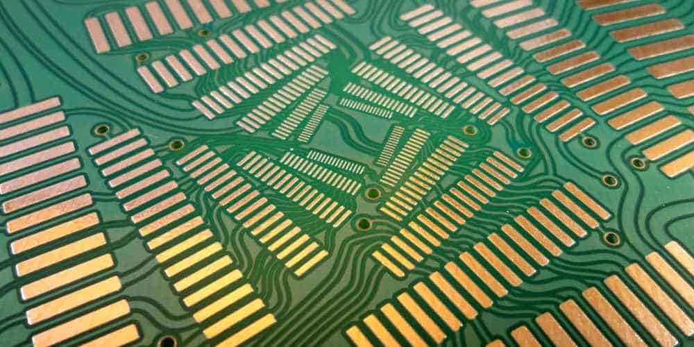
Visualizing the Copper Trace PCB
This formula can’t be revealed and analyzed without first knowing what a regular electronic board looks like, at least superficially. The typical thickness of copper on a circuit board is between 0.009 mm and 0.38 mm. The standard for PCB traces is either one ounce or 0.03 millimeters in height.
The Copper Trace PCB Resistance Equation
We can now give the equations and link this together because we have a firm grasp of what a typical electronic circuit looks like. Any conductor can be determined using the formula R = P*Area. The following values are assigned to each variable:
Resistance is represented by the symbol R.
P = the material’s resistivity.
The pure copper resistance at 25 degrees Celsius can be calculated using this formula.
At this temperature, the resistivity of pure copper is 1.724. With this information, we can calculate the area resistance, which is between 6 and 10 ohms per square centimeter.
Another instance: Let’s pretend the area is 0.375mm2. Multiplying this by the value of resistivity gives us a value of twenty ohms per centimeter or a resistance of hundred ohms. It’s a relatively small number, but the imperfection of the formula means it has the potential to cause considerable variation. It’s one factor that can influence how precisely PCB tracing measurements can be taken.
Using the Copper Trace PCB Resistance Equation
This phenomenon can also occur in power system current sensing systems that rely on resistance. The system will read 1100 ohms of resistance instead of the recommended 1000 ohms if a one-ohm sensing resistor is used with the 0.025 mm trace. That’s a big disparity, and it can cause the currency to drop in value more than is desirable or even necessary.
It is possible to manipulate the trace width without resorting to elaborate math. You might think about these alternatives to more time-consuming calculations. Instead of calculating the trace width on the PCB, you may just have a look at these alternatives.
If you want to check what kinds of circuits are properly linked to them, you can perform the first by just observing the width and raising or decreasing it. It’ll accomplish a couple of different things. First, it will expand the copper area, providing more wiggle room to try out various resistance values. And secondly, it will lessen the copper’s resistance on the board. Furthermore, it will provide additional room for testing to establish an appropriate trace width.
This can’t be done with packages containing a grid array. Another approach is to utilize a thick layer of copper and install it alongside the existing circuit board. The resistance will go down as the area goes up. One thing to keep in mind is that utilizing a thick layer of copper will necessitate investing in the necessary supplies to make a stickier copper coating. Spending money is required.
Why calculate Copper Trace PCB width?
A simple calculation or procedure may not be able to accurately detect the trace resistance, and calculating a typical PCB trace may not be enough. However, proper calculation of the trace widths and trace is required to guarantee proper activation of the PCB traces. Any given PCB trace’s resistance can be reduced by calculating and considerably increasing the width of the trace.
Conclusion
The provided data on PCB Trace should prove to be useful, I hope. Commonly referred to as “PCBs,” they comprise the backbone of many electronic gadgets and devices. When planning a PCB, it’s important to remember a few things.
