The design phase of the printed circuit board production process proves one of the most critical stages. It forms the basis besides kick-starting the entire chain of the circuit board production process. But as always, time becomes of the essence when it comes to getting the circuit board to the market. You do not want anything but to get the design details right from the beginning. One key way entails using a suitable PCB design software in developing the PCB layout or schematic, among other important aspects.
PCB Design Process
The evolution of circuit boards has necessitated the gradual but unmistakable change in the design and manufacture of printed circuit boards. Unlike before, electronic basic circuit design software exists to help designers generate top designs for their PCB projects. But as a PCB designer, understanding the design process proves essential. Therefore, before getting into the best PCB design software, let us canvass the PCB design process.
Knowing the Electrical Considerations
The first step before embarking on designing a printed circuit board entails comprehending the electrical limits or parameters of your system. It should include voltages, current maximums, capacitance limitations, signal types, and shielding considerations. Besides a comprehensive net wire schematic and listing, other parameters should entail impedance attributes, location, and type of circuit connectors and components.
Developing the Schematic
It is a crucial step and entails developing the electrical-level design of your BARE PCB board‘s function and purpose. Remember, at this point, the mechanical representation has not set in yet.
Deploying a Schematic Capture Program or Tool in Developing the PCB Layout
In most instances, a suitable PCB provider like RayMing PCB and Assembly will collaborate with you or principal engineers in developing a schematic. Software platforms like Allegro, Altium, Mentor PADS become instrumental in demonstrating the functionality of the board. It also depicts the locations of electronic components such as transistors. After creating the schematic, it becomes prudent for the engineer (mechanical) to load and determine how well the pcb pattern design will fit into the targeted application device.
Designing the PCB Stack-Up
It is an important consideration early on during the design phase due to the potential impedance. Impedance means the extent and how fast electricity can flow or travel down a copper trace. Stack-ups always play a pivotal role in determining how the engineer designs and fits the printed circuit board into the electronic device.
Defining Design Rules and Needs
The process step gets primarily defined by the acceptability criteria and standards of the IPC. IPC is instrumental in regulating quality standards in the PCB and electronics industry, especially when it comes to manufacturing. Such standards detail everything needed to understand the manufacturing of printed circuit boards. It is, however, always important to get a PCB layout company capable and familiar with such standards (IPC). It helps when it comes to averting project delays or major PCB project revisions.
Placing Electronic Components
It represents a collaborative stage. The PCB provider and the customer discuss the design besides the layout guidelines for component placement. For instance, the available standards or stipulations may indicate the non-viability of having specific components located near each other because of electrical noise generation in the circuit. The PCB solution provider will, in most instances, have the relevant data sheets relating to each component. Such then get placed within the mechanical layout before getting sent to the client or customer for consent.
Drill Hole Insertion
It is a step that gets dictated by the connection and type of components. For instance, almost half of the available flex circuits prove double-sided. It implies that a connection exists at the bottom layer (where it connects the hole)
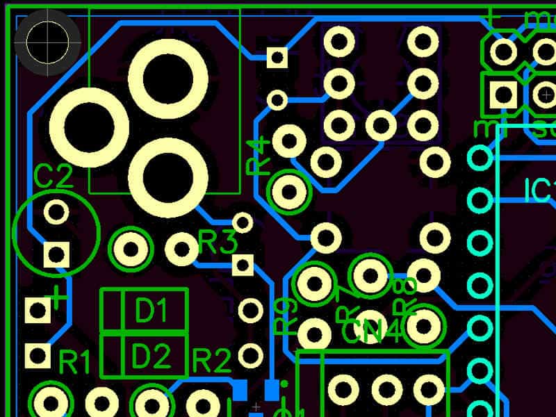
Routing of Traces
It follows the drill hole insertion phase and placement of drill holes and components. Routing of traces implies the connection of sections of the conducting path.
Incorporating Identifiers ad Labels
The process steps entail the incorporation of any identifiers, labels, reference designators, or markings to the circuit layout. Reference designators become helpful in illustrating the specific components or parts and locating them on the circuit board.
Generation of the Layout or Design Files
It is the ultimate step in the design or layout process—files containing all the relevant details of the PCB get generated. The generation of these files also signifies that your printed circuit board is ready for production (manufacturing and assembly).
Top 10 PCB Design Software
As a printed circuit board design enthusiast, hobbyist, or engineer, getting and acquainting yourself with relevant PCB design software becomes pivotal. However, finding a suitable printed circuit board design software can become a difficult task. It stems from the variety of design suites available for utilization. Failure to get and use the right software in designing your printed circuit board can lead to a costly failure. But specific attributes distinguish an excellent circuit board drawing software from the rest. If you want a top PCB design software, consider the following.
Attributes of a Top PCB Design Software
Schematic Capture
The PCB design software needs to have the provision of starting the design process from the schematic stage. It equally proves useful for complex and straightforward PCB designs, especially when you want an error-free board layout.
Automatic DRC
The PCB design software needs amenability regarding aspects like getting it to check for direct rule compliance for both complex and simple printed circuit board designs.
Backward and Forward Annotation
The circuit board design suite should allow for a backward and forward annotation as the board’s direct laying proves more arduous than starting with a circuit diagram to pcb converter software. It also forms a fundamental requirement for all types of PCB designs.
Assisted Routing
The design software needs to possess assisted routing as an essential requirement, especially for simple boards. However, it is not a requirement for complex boards as it can get accomplished manually without any assistance.
Auto-routing
The provision of automatic routing becomes essential for complex board designs. It is therefore vital to consider this aspect before selecting a suitable PCB design suite. But remember, simple boards can get routed manually.
Auto-placement
Depending on the PCB you intend to design, getting a PCB design software that allows for the automatic placement of components can prove helpful. It mainly applies to complex boards needing lots of electronic components. However, whenever the number of components proves few, it may not necessarily apply.
Real-time Component or Parts data
For PCB designs with large components, getting a design software that can track and avail the required data proves helpful. For a more straightforward board design that needs a few components, it is possible to manually research and gets the required component’s data without much fuss.
Export Options
A top PCB design software has to have the provision of at least exporting Gerber files. However, the broader the range of formats the software program provides, the better your design needs. Such an ability is a vital aspect to consider before picking a PCB design suite.
DFM Importation
It also depends on the type of printed circuit board you want to design. However, complex PCBs require more stringent specifications that align with industry needs. Additionally, such specifications have to align with the contract manufacturer’s equipment capabilities. Simpler PCB designs can get away with general industry standards regarding DFM (design for manufacturing)
Signal Analysis
A top PCB design software needs to analyze signals, primarily if your design features multiple types of signals at different frequencies. However, for simple circuits that have singular signal types and maybe a PDN, such a capability does not apply.
Thermal Analysis
The thermal analysis becomes a crucial aspect for complex circuits requiring thermal distribution and dissipation. Such printed circuit boards involve high power with diverse signal types. However, for simple circuits, the materials used often come standard, and thus, such a capability becomes optional.
3D visualization
The ability of the PCB design suite to visualize in three-dimension becomes crucial for complex circuit diagram to pcb design software. It especially applies when you have integrated MCAD. However, the capability proves unnecessary for simple PCB designs, especially double and single-layered PCBs.
ECAD to MCAD Integration
The printed circuit board software design has to integrate ECAD to MCAD, especially for complex boards. It allows for exact board dimensioning when it comes to installation. Simple boards, however, do not require this as they do not encompass enclosure integration.
Panelization Design
It is essential to have this capability in the design software of choice. It allows for the specification of the depanelization approach used in complex boards. The importance of having this feature dissipates when dealing with simple boards.
Comprehension of the design process is instrumental before picking a suitable and top-tier design software to use. So what happens next? You have to pick a top printed circuit board design software. The following section will cover some of the famous and top PCB design software to consider.
Top Ten PCB Design Software
#1. Altium Designer
Altium Designer is one of the most trusted PCB design software systems world-over. It allows designers and engineers to connect with each aspect of the printed circuit board design process. The software has involved over thirty-five years of constant development and innovation. It provides a unified design environment that resonates with many and is famous as a circuit board design solution. However, it would help if you bought it at a starting monthly price of USD 325.
Features
- Design reviews. It is instrumental in making the software successful. It allows users to capture design deliberations via contextual commenting in the Altium Designer or the web browser. As a result, the feedback gets recorded and acted upon effectively.
- Electronic collaboration. It is an attribute that allows users to work with others in collaborative efforts from across the world. As a result, the Git-based version control, besides visual differencing abilities, will enable designers to stay in sync every time.
- Customer Interaction. The feature allows you to update your client or customer by sharing regular design snapshots (work’s progress). What’s more? Such progress can get accessed from anywhere provided the device can access a web browser.
- Manufacturer Collaboration. It allows for production data release and enables your solution provider to view and remark on your manufacturing output.
- MCAD Collaboration. The feature is instrumental in maintaining synchrony with mechanical engineering fellows. It achieves this through bi-directional and file-less collaboration.
- It also allows for software collaboration, especially in debugging hardware, remote work, and anonymous information sharing.
- Other crucial features include an embedded viewer, a unified interface, global editing, interactive routing, easy-to-use intuitive feature, etc.
#2. EasyEDA
It comes as a web-based EDA software tool that is instrumental in helping engineers to simulate, design, share (both privately and publicly), and discuss the PCB schematics, PCBs, and simulations. The design software comes as an open-access tool available to everyone with interest. EasyEDA provides access to every core function and necessary tools for the design of printed circuit boards. It also possesses an incredible set of innovative attributes. You can work on schematic capture, project management, library management, design, team collaborations, etc.
Features
- Libraries with more than one million updated components
- An LCSC catalog that details pricing and other relevant details of more than two-hundred thousand electronic components.
- Web-based functionality
- Format compatibility
- Image-to-shape conversion
- Auto-routing function
- A functional and straightforward user interface
- SPICE simulation
- Team collaboration
#3.Eagle PCB
Also referred to as Autodesk EAGLE, Eagle PCB is a popular EDA platform fully published and owned by Autodesk. The acronym EAGLE refers to Easily Applicable Graphical Layout Editor. It is a capable design software with various tools ad options to handle complex PCB projects. The software got developed and released by Cadsoft in 1988, though acquired, enhanced, and released by Autodesk in 2016.
As a user, you enjoy getting a project manager, a multi-window GUI (graphical user interface), and design reusability utilities. It all gets accompanied by other innovative attributes that permit a productive and efficient design process. The current EAGLE version (9.6.1) can operate on Linux, Mac OS X, and Windows devices. It is also available in multiple languages with different pricing plans that tally with different user requirements.
Features
- DDS or dynamic design synchronization, which is instrumental for large and complicated PCB design projects.
- Autodesk design platform, a trusted platform that also operates in other programs like Inventor, AutoCAD, etc., provides a whole EDA and CAD/CAM design solution that processes diverse design needs.
- Enhanced routing technology
- The latest EAGLE version provides an enhanced interactive manual besides an automatic routing experience. An excellent example entails the OAR (obstacle avoidance routing) system that detects obstacles and routes around them. It also has the option for auto-rerouting.
- Design for High-Density Interconnect structures. HDI has increasingly become important with the emergence and demand for compact PCBs. It has a large PIN, BGA, and high frequencies escape routing.
- Rule checking attribute
- SPICE simulation
- PCB library content
#4. PCB Creator
It is a highly rated PCB layout software option. The design software comes as open access or free design software product complete with simple features. PCB creator provides a smooth upgrade path for unlocking the ability required for complex PCB designs. It also allows for custom PCB orders for fabrication within the software program.
Features
- Reliable as well as friendly. The design software product has an intuitive UI besides high flexibility to reduce company losses. Customers can instantly become productive by using this software program.
- A smart project arrangement. The PCB design software proves convenient for both complex and straightforward PCB projects. Nets get divided with net classes besides having user-defined limits and class-to-class regulations. It becomes possible to apply the design rules of a specific project to another board project without specifying them all afresh.
- Integrated environment. The software modules make up the printed circuit board design environment besides management of the module library and simple access to the net or previous design phases. It also allows the schematic conversion into PCB and renews the printed circuit board from the schematic besides back annotation.
- Multi-level hierarchy. It is possible to insert hierarchy blocks into the main schematic sheet. Additionally, users can directly arrange components into the hierarchy blocks located on the circuit board besides applying routing and placement from a single block to the other.
- 3D preview. The feature allows the rotation of the board in the three possible axes. It also allows real-time zoom-out/zoom-in function besides adjusting the preview’s color template. The board can get exported to RML 2.0 or STEP formats that get supported by CAD systems.
- Placement features. The feature allows for the automatic or manual placement of components with optimized pad distances.
- Built-in auto-router is suitable for complicated multi-layer circuit boards possessing buried/blind and through vias.
- Other features include manual routing, import/export, fanout, comprehensive libraries, manufacturing output, etc.
#5. Cadence Allegro
The design software suite is well-rated and helps in bringing the innovative PCB designs alive. It has a comprehensive, easy-to-use, and powerful suite of program tools capable of effortlessly tackling both complex and simple projects. The design environment the software provides offers real-time and visual feedback. It also ensures the manufacturability and functionality of the printed circuit board while cutting on the design time.
Features
- Simple-to-use suite tools
- Provides a constraint-driven design environment
- Routing and layout algorithms
- Team or collaborative design features
- Real-time manufacturability or production checks to limit the design iteration number
#6. KiCad PCB
It is popular open access or free design software suite for automated electronic design. KiCad facilitates the designing of PCB schematics besides the conversion of printed circuit board designs. The design software program got developed by Pierre Charras and featured an intriguing integrated environment for PCB layout design and schematic capture.
Features
- Schematic capture. It has a schematic editor to help develop PCB designs without limitations. The KiCad lacks paywalls that mostly unlock features, though it has a standard library of schematic symbols. It also has the schematic symbol editor to assist you in getting to speed with your PCB designs.
- KiCAD has a three-dimensional viewer that can inspect PCB designs on a canvas (interactive). You can pan around or rotate the design to review specific details impossible to discern in a two-dimensional view. Additionally, numerous rendering alternatives allow for the aesthetic modification of the circuit board. It can also show or hide features to allow for a more straightforward inspection process.
- A push-and-shove router. It proves adept at routing distinct pairs besides interactively tuning the trace lengths.
#7. OrCAD PCB
The OrCAD designer comes as a comprehensive PCB design solution with advanced route and place technology. It is a tiered and scalable design software that delivers cutting-edge capabilities besides a highly integrated flow. Some of the aspects of OrCAD PCB designer include librarian tools, schematic capture, PCB routing and editing, constraint manager, auto-routing, signal integrity, and optional mixed-signal PCB simulation.
Features
- Intelligent route and place that maximizes productivity with intelligent interactive and automatic etch editing besides placement.
- Future-proof scalability that maximizes your investment by understanding the products and design technologies can grow.
- ECAD-to-MCAD integration with SolidWorks
- Interactive three-dimensional canvas
- Segment over voids to detect cline segments
- Static to the dynamic shape
#8. Protel PCB
Protel PCB has a huge reputation as top PCB design software among electronic engineers and designers. It is instrumental in designing PCB layout, retrieving previous circuit board designs from the archives, and confirming schematic designs.
Features
- Advanced place and route tools that act as its signature feature
- Enhanced functionality and utilities that helps designers to stay competitive
- Unified interface
- 3D visualization
- Customer interaction
#9. PCB123
PCB123 from Sunstone is a popular and superior PCB design software that provides comprehensive tools from conceptualization to manufacturing. The application not only comprises PCB schematics but PCB layout within a unified database. It does not require a netlist as the interface connecting the applications.
Features
- The capability of creating a multi-paged schematic that uses symbols representing complete components or part sections like a gate
- Presence of a component or parts database structured in a taxonomical manner
- Fully defined parts libraries with over 750000 components complete with footprints, schematic symbols, Digi-Key, and manufacturers
- Auto-router feature for unrestricted access to routing layers
Final Remarks
A PCB design software is instrumental in the modern-day design and fabrication process of printed circuit boards. As an electronics designer or engineer, understanding the diverse top alternatives of PCB design software comes in handy in ensuring quality printed circuit boards.
