If you are new to PCB design, it may be helpful to review the basics of the circuit board layout. We will go over the most important PCB design rules and how to balance your trace lengths and components on a board. You will also need to know which components you should isolate to keep their temperatures low. For example, you should separate high-power components from each other to even out their temperatures. To calculate this, look up the thermal resist rating of the component. You can use this information to decide whether you need to use heatsinks or cooling fans to cool them down.
The stack-up definition is a fundamental component of PCB design. It describes the physical structure of the multilayer circuit board, such as the amount of copper used in each layer. It is vital for manufacturing the circuit board, as a correctly stacked board helps minimize crosstalk and electromagnetic emissions. This also improves signal integrity. Stack-up also defines how there is interconnections of components. For example, if traces are too close to each other, they can lead to a poor signal integrity.
Placement is another key step in PCB design. It involves strategic assessment of the board’s real estate to minimize layers transitions. Placement should adhere to specific design rules to ensure optimal routing. You must follow several design principles to avoid mistakes. Make sure that component placement is within the specifications required for the printed circuit board. For example, a PCB design should be 0.02 mm larger than its nearest neighbor. You can construct a PCB design with fewer errors and a lower cost by following these guidelines.
PCB Design Resources
There are many resources to help you with PCB design. You can attend blogs and industry conferences to learn the ins and outs of design and production. You can also hire a PCB contract manufacturer for design, engineering, and manufacturing expertise. These firms can help you explore new technologies and help you overcome common design challenges. They will also provide you with specialized components and services. You should always have a budget cushion.
A PCB is the heart of any electronic gadget or electrical device. High-speed electrical connectivity is essential. Integra Sources can help you with every step of the design process. With their dedicated hardware engineers, you’ll control costs and scale your project accordingly. No matter what type of electronics product you’re building, you’ll need a PCB. Integra Sources’ comprehensive solution for PCB design includes PCB layout and design consulting.
CAD software and Gerber viewer are two of the most essential PCB design resources. These software programs are indispensable in the process, and most of the time spent in the CAD phase is spent on PCB layout. In addition, Mentor Graphics PADs and Orcad Capture are industry standard tools. These resources are especially helpful if you are just starting out. However, the resources mentioned above are not exhaustive. You can find many more PCB design resources, including books and blogs.
Consumer electronics require small PCBs with high-volume connections. In addition to this, consumer electronics require low-cost PCBs. However, despite the high demands of PCB design for these products, these manufacturers need reliable boards to make their products function well. With the help of PCB design resources, your medical devices will become more advanced and functional. The medical sector is continuously coming up with new uses for electronics. As technology improves, the possibilities for smaller, denser boards will increase.
Your Guide to PCB Design Basics & Steps
PCB design is a complex process that requires careful preparation, which is why Your Guide to PCB Design Basics abounds in valuable advice. It starts with a schematic, which is the electrical design but has not yet undergone translation into a mechanical representation. The schematic capture tool will create a PCB layout based on this electrical design. The schematic capture tool is essential for PCB design because incorrect symbols make the entire process difficult.
When designing a PCB, you’ll first want to decide the size of the board. The enclosure that houses your PCB will often be the largest limiting factor. Besides enclosure size, component selection can also affect the size of the board. For example, surface-mounted components have a low-profile, so they can be made smaller. By contrast, through-hole components have larger footprints and are easier to find and solder.
The layout of your PCB will depend on where you’ll place the components. For example, suppose you’re designing an audio amplifier. In that case, you may want to place the power switch near the volume potentiometer so that the LED will indicate whether the power switch is on. However, larger circuits are more complex, and a single copper layer may be insufficient. Often, two copper layers will be necessary, and traces will need to be routed on both sides of the board.
Once you’ve made your PCB layout, you’ll need to print it out. Remember that these blueprints don’t print on an 8.5 x 11 sheet of paper, but on a plotter printer. This plotter printer prints the PCB design as “film. ” This film is similar to the transparencies you might have seen in school. It’s like a photo negative of the board. Remember that clear ink represents copper pathways, and black ink indicates areas you will remove.
General Considerations on High-Power PCBs
If you are planning to design a PCB for a high-power device, there are some general considerations that you need to consider. These factors can be crucial to ensure that the board is designed correctly and functions properly. In this section, you will learn some of these important tips. Also, you will learn how to design high-power PCBs. Keep reading to learn more! Below are some of the most important factors to consider when designing a PCB for high-power applications.
First and foremost, the PCB design should incorporate fuses and other safety features. Fuse holders are important for protecting against short-circuiting, but you should also consider other design features. For instance, you should consider the manufacturing process of a PCB and the quality of the materials used to produce it. In addition, a high-power PCB must withstand the voltage applied to it. Moreover, a high-power PCB must have a failsafe firmware that can detect the increase of temperature. Moreover, the PCB design should contain components with low resistance to avoid short-circuiting, which poses a risk for a human.
The number of years in the PCB manufacturing business also determines the quality of high-power PCB. Experienced manufacturers will probably be equipped with the necessary equipment and manpower to produce high-power PCBs. Nevertheless, not all PCB manufacturers can fabricate high-power PCBs. Similarly, companies with limited prototyping and production facilities may not have the manpower to handle these complex PCBs. Considering all these factors, it is best to find a company that can provide both.
PCB Surface Finish Types
PCB Surface Finish Types include tin, gold, and immersion. Immersion tin is the most affordable type of immersion coating, but it does have a few disadvantages. For example, immersion tin is not compatible with projects that require a removable solder mask. This type of surface finish is also not very popular for small quantities of PCBs. Listed below are the pros and cons of each surface finish.
Before choosing a PCB surface finish type, determine the production volume that you need the PCBs for. Also, consider the environment in which your PCBs will operate, since different finishes can be susceptible to environmental impacts. A skilled team of electronics manufacturing services can help you choose the right surface finish. If you are unsure, contact a manufacturer to request a free quotation. You can also request a quote online to get an idea of their prices.
Gold-based finishes are popular in electronic assemblies, including miniature and lead-free components. These PCBs are extremely high-speed and have high-reliability requirements. ENIG, for example, is highly affordable and has good solderability. Other PCB surface finish types may base on a particular technology or requirements. HASL, for instance, is aerospace approved. However, it is important to note that there are various benefits to each of these finishes.
ENIG is a double-layer metallic coating that protects copper and provides a level exterior for complex surface components. RoHs regulations have increased the use of ENIG. ENIG is not always cost-effective, but is highly protective and offers superior electrical and mechanical properties. There are also many disadvantages to ENIG. However, ENIG is the most widely used PCB surface finish. It is also one of the most environmentally friendly.
Controlled Impedance Design Guide
The Use of a Controlled Impedance Design Guide is critical to the high-speed performance of your circuit board. The design of a PCB using controlled impedance is crucial to high-speed signal processing and computer video. The PCB’s signal traces behave like transmission lines, and the impedance of each varies from point to point. The higher the difference, the more likely the signal is to be reflected. The reflected signal will travel in the opposite direction, superimposing itself on the main signal.
The use of a Controlled Impedance Design Guide involves selecting an Impedance Profile and creating a routing rule based on that profile. Once the design is complete, click OK to save the project. The resulting file will have a simulated return path for the signal NetX. You can also configure the DRC to display the signal path in a Violation Display Style, which highlights the violation location.
The Controlled Impedance Design Guide is the ideal tool for communicating your expectations with your circuit board manufacturer. The guide includes an interactive interface that can help you understand the intricacies of controlled impedance, including the rules of use and calculating the impedance. It also outlines the steps involved in creating a design and the final product. The Controlled Impedance Design Guide is essential for all PCB manufacturers.
Controlled Impedance Design Guides help your customers create the best possible PCB. They also help you determine the best way to communicate your customer’s simple or complex requirements. Listed below are the main benefits of using a Controlled Impedance Design Guide. So, if you’re looking for the perfect guide for your next project, the Controlled Impedance Design Guide can help you get the best results.
PCB Routing Tips
PCB routing is an important process in the creation of electronic circuits. However, if you do not design a circuit board properly, it will be useless, inefficient, and slow. By following a few PCB routing tips, you can avoid such problems. The following are some of the most crucial PCB routing tips. Follow these guidelines carefully to achieve optimal routing. The result will be a circuit board that is aesthetically pleasing and fully functional.
First, you must study the schematics to know how to route components in a specific way. Print the schematic out or view it on a second monitor to see the components. Decoupling caps, for example, should be placed next to the IC to prevent their short circuit. It is important to understand the schematic and space values required to connect the circuit components for better PCB routing. The circuit board routing should be accurate and easy to read.
Another PCB routing tip is to consider the signals on the printed circuit. Keep analog signals separate from digital ones. Digital signals travel on parallel traces, which can cause capacitive couplings. This interference between the signals is difficult to solve without making changes to the PCB. If you’re unsure of the signal line requirements, consult an engineer for guidance. Remember to keep the signal lines in their proper order. Then, use a routing tool with the right constraints to complete the process without any issues.
The Importance of PCB Vias
PCB vias are the most important part of your design when it comes to manufacturing. Vias are a simple pair of drilled holes separated by a pad. Sizes of the holes and pads depend on the size of the board. Smaller vias are more flexible, allowing more space for traces, but they also cost more. Therefore, during the layout stage, you should take time to plan the via design, and submit it to the factory.
PCB manufacturing requires the use of vias in order to make electrical connections. These holes are drilled with certain tolerances, and you may also manufacture them off-location. Therefore, allowances for drill position errors are necessary before manufacturing. Without proper vias, manufacturing yield is reduced. In addition, regular through hole vias must be plated. Various processing steps are needed to ensure that the through holes are plated properly. The result is a layer of thin orange and gray materials that makes the electrical connection.
PCB vias are made with several different types of materials. In addition to conductive material, they can also be made with a copper core. The first type is made of copper. It is essential when the board must be a high-reliability product. Another type is made of plastic. Plastics are generally more expensive than metal, and may be more sensitive to abrasive materials. PCB Vias are available in a variety of shapes, including circular or angled vias.
How to Learn PCB Designing
If you have been thinking about becoming an electrical engineer but haven’t had the chance to learn PCB designing, you’re not alone. Electrical engineers need to know how to create circuit boards for many industries. While their educational training may not have focused on PCB design, there’s a need for young, creative designers to join the field. In addition to the manufacturing industry, PCB designers are needed in various R&D groups and industries across the world. Once you get enough experience and the right skills, you’ll build a career in a variety of different fields.
If you’re unsure of where to start, you can always try an online course. To learn PCB designing, you need to know the basics of PCB composition and the use of an EDA software. PCB design can be a lucrative career for engineers who are skilled in using EDA software. With enough motivation and practice, you can become an expert in the field. You need a good EDA software package and a willingness to learn. You can also start from scratch by following a tutorial or two.
What is Artwork in PCB Designing?
PCB designs need to be based on the correct artwork. We use this artwork to create the pattern of printed wires and components on the board. It is similar to printing plates, but is only vaguely related. The artwork will define the size, orientation, and composition of the board’s components, solder pads, and lands. It must also show true to scale measurements and any scaling level that is required. Therefore, PCB artwork is crucial to the successful manufacture of a circuit board.
When creating an image for your PCB, you must make sure that it is in SVG format. The artwork scale gives you the relative accuracy of the scaled image compared to the PCB area. For instance, a 2:1 artwork scale would be four times as large as the PCB’s surface area, and a 4:1 artwork would be 16 times finer. The ratio should match the actual area of the PCB.
The artwork generated for single-sided printed circuit boards is simple. However, the artwork generation for a double-sided board involves a bit more work. You make double-sided PCBs using two metal layers. Each layer has holes, which link components and details on one side to one on the other. When you design a multilayered PCB, your artwork will require more layers, making it more expensive and time-consuming.
Can You Design PCB in AutoCAD?
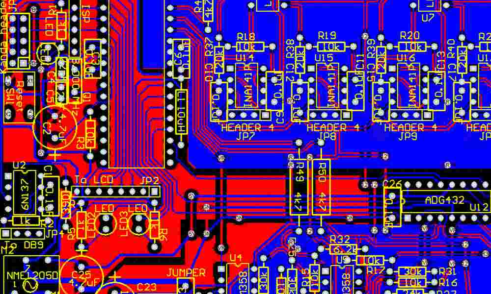
When designing a circuit board, you’ll need to create a grid that allows the layers to fit together. This is called a solder mask. It is important to remember that a rectangular grid does not always fit together properly, and there’s no such thing as a square grid. For example, a PCB comprises two copper layers, one red and one blue. The copper layers are strategically routed and the shapes are called vias. Vias are yellow circles that pass a signal from one side to the other. They can be bigger than normal to accommodate through-hole parts. In addition, other hidden layers will reveal copper.
While there are many programs for PCB design, AutoCAD is a powerful tool for professional designers. This tool is intuitive and easy to learn, making it ideal for beginners. It allows you to create 3D designs with ease. Moreover, learning AutoCAD will help you broaden your knowledge and skill in design. This software can be a great addition to your computer. So, get your hands on AutoCAD and make your next project a success!
You can also create a part library in AutoCAD using the Block attribute. In AutoCAD, a block is a text string that we can define as a variable. Once you insert the block, you get a prompt to type the desired text string. This feature is especially useful for adding component values and reference designators. Make sure that the block you’re inserting is on the correct layer. Otherwise, the data won’t appear in the right place.
Advantages of Surface Mount Components in PCBs
Traditionally, electronic components were mounted and soldered into place on circuit boards. These electronic features included transistors, resistors, and capacitors. While it was possible to place these components manually, most manufacturers today use special machines. These machines create more accurate, high-quality results. Here are some of the reasons that manufacturing companies prefer surface-mount components. First, they are much more compact and flexible than wired components. This makes them ideal for automated pick and place machines.
A typical PCB contains several types of surface-mount components. The first type is a resistor, while the second type is a capacitor. Resistors are small rectangular chips with or without numbers. A common surface-mount package size is 0603 (1608 metric), while a ferrite bead is slightly larger at 0805 (2012 metric). On the other hand, a MOSFET transistor is about the size of a British postage stamp.
Another option is the use of through-hole technology. This type of technology uses holes instead of a drilled hole in the PCB. The result is a much more accurate surface-mount product. Using this technology has many advantages, including reduced cost and increased reliability. For example, it makes it easier to automate assembly and soldering, which increases the productivity of electronic devices. And unlike through-hole technology, a PCB with surface-mount components is much easier to manufacture.
As far as the size and weight of surface-mount components is concerned, they are usually smaller than their lead-based counterparts. This makes them easier to handle and transport. Using a machine to handle them is also easier, as the leads of SMT devices are typically a lot smaller. In addition, the shape and size of these components are standardized in the electronics industry by the leading standardization body.
How to Design a PCB Layout
If you’re wondering how to design a PCB layout, this article is for you. If you’ve never done it before, you’ll be glad to know that it’s not as complicated as it looks! Whether you’re a newbie or a pro, there are several things that you should know. Follow these tips and you’ll be on your way to designing your own PCB!
First, you must decide which components you’re going to place on the PCB. For example, you might place the power switch near the volume potentiometer. For larger circuits, you may want to use two copper layers and route the traces on both sides of the board. It’s also a good idea to label the components so that you can see their labels when complete.
Creating a PCB layout is one of the most important aspects of designing an electronic device. It allows you to place electronic components on the board while securely connecting their terminals. Without a proper PCB layout, your device wouldn’t work. While engineers spend hours and even days creating the perfect PCB layout, anyone can learn to design the right PCB layout. After all, a professional designer can save you a lot of time and money by using the expertise of an experienced PCB manufacturing company.
You should also know the size of your board. A good PCB layout must be large enough for all the necessary components. The size of the board will depend on the functionality and size of the final product. Because electronic products are getting smaller every day, this aspect of PCB design is increasingly important. Moreover, you should estimate the size of the PCB. Then, consider the size and shape of the enclosure. In some cases, multilayer circuits or high-density interconnects may be required.
How to Go From PCB Schematic to Board Layout
If you’re designing a circuit board, you may wonder how to go from PCB schematic to board layout. After all, the PCB schematic is the basis for the board layout. As such, it’s important to ensure that you follow the design rules and seamlessly import any changes made in the schematic into the board layout. Altium Designer can help you with the synchronization process, as it includes design tools that keep the schematic and board layout in sync. And with Altium Designer, you can eliminate the need for an external schematic capture program.
Before starting the layout process, it’s a good idea to review your PCB schematic. It will likely undergo several revisions before going into production. Checking it now can help you avoid surprises during the board layout. In addition, it can help you find duplicate circuitry, and parts that you may have forgotten to remove. Regardless of your background in electronics, you’ll benefit from the extra attention to detail. Besides that, a PCB schematic is a great way to avoid rushing through a design stage if it’s not completely final.
CAD software works to convert a completed schematic into a realistic PCB layout. In this stage, the schematic consists of component footprints, ratlines, and electrical connections between components. A designer then arranges these components and utilizes the ratlines to draw traces, vias, and copper pours. We identify a via as a small through-hole carrying an electrical connection to another layer of the PCB. It may also serve as a thermal via that connects to an internal ground plane.
PCB Layout Capabilities
PCB layout is an essential aspect of electronic manufacturing. If not done correctly, it can result in electromagnetic interference, conflicts between components, limited board functionality, or even complete product failure. Improper PCB layout can be costly and cause delays during the manufacturing process. A professional PCB layout company can help you avoid these problems. Below are some of the key factors to look for in PCB layout software. Let’s take a closer look.
PCB layout software enables designers to simulate layouts to ensure the right placement and routing of components. By calculating the optimal length for conductive tracks, engineers can optimize the board layout and ensure the proper placing of components. For example, the length of the conductive trace affects the amount of radiation a device will produce and its susceptibility to electromagnetic interference. In addition, the longer the conductive track, the greater the chance of interference and quality impairment. A good PCB layout software allows designers to simulate the length of the signal track.
With its advanced layout capabilities and collaboration features, PADS PCB design solutions can streamline the design process. The company’s multiple teams can use the software to consolidate inventories, component orientations, and manufacturing requirements, accelerating the development process. In addition, Xpedition uses industry-approved mathematical algorithms to enable designers to easily view and modify part libraries with the appropriate dimensions and orientations. It also calculates footprint dimensions from dimensional data and builds standard SMT library parts in minutes, which can help minimize time-to-market.
