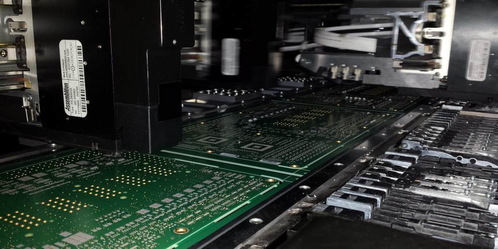
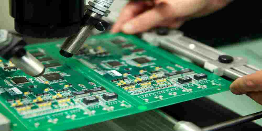
Printed circuit boards (PCBs) are an essential component of many electronic devices, including smartphones, computers, and automobiles. As electronic devices continue to become smaller and more complex, the need for reliable and efficient PCBs has become increasingly important. One of the challenges associated with PCB design is electromagnetic compatibility (EMC), which refers to the ability of a device to function properly in the presence of electromagnetic interference (EMI).
EMC is a critical consideration for PCB designers, as EMI can cause a range of issues, from reduced performance to complete failure of the device. EMC testing and compliance are also becoming more stringent, as governments and industry organizations seek to ensure that electronic devices are safe and reliable. To achieve EMC, PCB designers must consider a range of factors, including the layout of the board, the placement of components, and the use of shielding and filtering techniques.
In this article, we will explore the topic of EMC for PCBs in more detail, including the challenges associated with achieving EMC, common techniques used to address EMI, and the importance of EMC testing and compliance. By understanding the principles of EMC for PCBs, designers can create reliable and efficient electronic devices that meet the needs of consumers and regulatory bodies alike.
What is EMC?
EMC Definition
EMC stands for Electromagnetic Compatibility. It is the ability of electronic devices to function properly in the presence of electromagnetic interference (EMI) without causing interference to other devices. EMI can be generated by various sources such as power lines, radio and TV broadcast towers, mobile phones, and other electronic devices. EMC is essential to ensure that electronic devices can coexist and operate correctly in the same environment without causing interference to each other.
Why is EMC important for PCBs?
EMC is crucial for printed circuit boards (PCBs) as they contain various electronic components that generate and receive electromagnetic signals. PCBs are used in a wide range of electronic devices, including computers, mobile phones, medical equipment, and automotive systems. If a PCB is not designed to be EMC compliant, it can cause interference to other devices and malfunction in the presence of EMI. Furthermore, non-compliant PCBs can fail to meet regulatory requirements, resulting in costly product recalls and legal issues.
To ensure EMC compliance, PCB designers must consider various factors such as the layout and placement of components, routing of traces, and shielding techniques. They must also use appropriate components that meet EMC standards and perform testing to verify the PCB’s EMC performance.
In conclusion, understanding and implementing EMC is critical for the proper functioning of electronic devices that use PCBs. By designing PCBs that are EMC compliant, manufacturers can avoid costly product recalls, ensure regulatory compliance, and provide reliable products to their customers.
EMC Design Considerations for PCBs

Grounding and Shielding
Grounding and shielding are essential to minimize electromagnetic interference (EMI) and radio frequency interference (RFI) in printed circuit boards (PCBs). A well-designed grounding system ensures that all components are at the same reference potential, reducing the potential for ground loops and noise. Shielding can be used to prevent EMI and RFI from entering or leaving the PCB, reducing the impact of external sources of interference.
Trace Routing
Trace routing is a critical aspect of PCB design for EMC. Proper routing of traces can minimize EMI and RFI by reducing the length of conductors and minimizing the loop area. Differential routing can also be used to reduce common-mode noise. It is essential to avoid sharp corners and right angles in trace routing, as these can cause reflections and increase EMI.
Component Placement
Component placement is another crucial factor in EMC design for PCBs. Placing components too close together can cause crosstalk and coupling, leading to EMI and RFI. It is essential to place high-speed components away from sensitive components and to keep analog and digital components separate. The placement of decoupling capacitors is also critical to minimize power and signal noise.
Power and Signal Integrity
Power and signal integrity are essential for EMC design in PCBs. Proper power distribution and decoupling can minimize power noise and reduce EMI. It is essential to avoid ground bounce and to ensure that power and ground planes are well-connected. Signal integrity can be improved through the use of controlled impedance routing and proper termination.
In summary, EMC design considerations for PCBs include grounding and shielding, trace routing, component placement, and power and signal integrity. By following these guidelines, designers can minimize EMI and RFI and ensure that their PCBs meet regulatory requirements.
EMC Testing for PCBs

Pre-Compliance Testing
Before sending a PCB for full compliance testing, it is recommended to perform pre-compliance testing to identify any potential issues that may cause the board to fail the full compliance test. Pre-compliance testing can be done in-house with the help of an EMC test setup, which typically includes an EMC analyzer, an antenna, and a spectrum analyzer.
During pre-compliance testing, the PCB is tested for its electromagnetic radiation and susceptibility levels. The test results are then analyzed to identify potential sources of interference and to determine if the PCB meets the relevant EMC standards.
Full Compliance Testing
Full compliance testing is the final stage of EMC testing for PCBs. This testing is typically performed by a third-party testing lab that specializes in EMC testing. The lab will test the PCB for its electromagnetic radiation and susceptibility levels and compare the results with the relevant EMC standards.
If the PCB passes the full compliance test, it can be certified as compliant with the relevant EMC standards. If the PCB fails the test, the lab will provide a report detailing the issues that caused the failure. The PCB designer can then use this information to make the necessary changes to the board to improve its EMC performance.
In summary, EMC testing is a crucial step in the design and development of PCBs. Pre-compliance testing can help identify potential issues before full compliance testing, while full compliance testing ensures that the PCB meets the relevant EMC standards. By following these steps, PCB designers can ensure that their boards are compliant with EMC regulations and perform reliably in their intended environment.
EMC Regulations for PCBs
FCC Part 15
The Federal Communications Commission (FCC) is responsible for regulating electronic devices in the United States. FCC Part 15 is a set of regulations that govern the unintentional emissions of electronic devices. The FCC requires that all electronic devices meet certain electromagnetic compatibility (EMC) requirements to ensure that they do not cause interference with other electronic devices.
For PCBs, the FCC requires that all electronic devices meet certain limits for radiated and conducted emissions. These limits are specified in FCC Part 15 and are measured in decibels per milliwatt (dBm). The limits vary depending on the frequency range of the emissions and the type of device.
CE Marking
The CE marking is a certification mark that indicates conformity with health, safety, and environmental protection standards for products sold within the European Economic Area (EEA). The CE marking is required for many products, including electronic devices.
For PCBs, the CE marking requires compliance with the EMC Directive. The EMC Directive sets limits for the emissions of electronic devices and requires that they meet certain immunity requirements to ensure that they are not affected by external electromagnetic fields.
To obtain the CE marking, PCBs must be tested by a third-party testing laboratory to ensure that they meet the requirements of the EMC Directive. The testing process includes both radiated and conducted emissions testing, as well as immunity testing to ensure that the device is not affected by external electromagnetic fields.
In conclusion, compliance with FCC Part 15 and CE marking requirements is essential for electronic devices, including PCBs, to ensure that they do not cause interference with other electronic devices and meet health, safety, and environmental protection standards.
Conclusion
In conclusion, EMC is a critical factor that should be considered when designing printed circuit boards. By implementing EMC measures, designers can ensure that their boards meet the required standards and regulations, as well as prevent any potential issues that may arise from electromagnetic interference.
There are various EMC measures that can be implemented, including filtering, shielding, and grounding. Choosing the right approach will depend on the specific requirements of the application, as well as the budget and resources available.
It is important to note that EMC is not a one-time consideration, but an ongoing process that should be reevaluated as the design evolves. By keeping EMC in mind throughout the entire design process, designers can minimize the risk of issues arising down the line.
Overall, implementing EMC measures may require additional resources and effort, but it is a worthwhile investment that can ultimately save time and money in the long run.
