Table of Contents
ToggleA full wave bridge rectifier is a crucial component in many electronic devices. It is responsible for converting an alternating current (AC) into a direct current (DC) by rectifying both the positive and negative portions of the AC waveform. The design of a full wave bridge rectifier printed circuit board (PCB) is critical to the performance and efficiency of the rectifier.
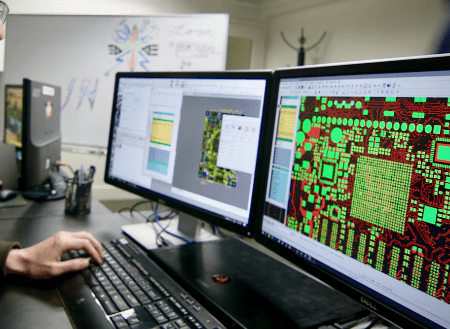
The PCB design of a full wave bridge rectifier involves careful consideration of various factors such as component placement, trace routing, and thermal management. The layout of the components on the PCB should be optimized to minimize the length of the traces and reduce the parasitic inductance and capacitance. The trace routing should be done in a way that minimizes the voltage drop and ensures that the current flows smoothly through the circuit. Additionally, the PCB should be designed to dissipate the heat generated by the rectifier to prevent damage to the components and ensure reliable operation.

Basic Principles
A full wave bridge rectifier is an electronic circuit that converts AC voltage into DC voltage. It is a vital component in many electronic devices that require a steady DC voltage supply. The circuit is composed of four diodes arranged in a bridge configuration, which allows the current to flow in one direction only.
The basic principle of a full wave bridge rectifier is that it takes the AC voltage and converts it into pulsating DC voltage. The four diodes are connected in such a way that they allow the current to flow in one direction only. When the AC voltage is positive, two of the diodes conduct, and when the AC voltage is negative, the other two diodes conduct. This results in a pulsating DC voltage output that has a frequency twice that of the input AC voltage.
The output voltage of a full wave bridge rectifier is not a steady DC voltage but a pulsating DC voltage. To get a steady DC voltage, a filter capacitor is connected to the output of the rectifier. The capacitor filters out the AC component of the pulsating DC voltage, resulting in a steady DC voltage.
The design of a full wave bridge rectifier PCB involves selecting the appropriate diodes and capacitors based on the required output voltage and current. The diodes must be rated for the maximum expected current and voltage, and the capacitor must be rated for the maximum expected voltage and ripple current.
In summary, a full wave bridge rectifier is an electronic circuit that converts AC voltage into pulsating DC voltage. The circuit is composed of four diodes arranged in a bridge configuration, which allows the current to flow in one direction only. To get a steady DC voltage, a filter capacitor is connected to the output of the rectifier. The design of a full wave bridge rectifier PCB involves selecting the appropriate diodes and capacitors based on the required output voltage and current.
Components of Full Wave Bridge Rectifier

A full wave bridge rectifier is a circuit that converts AC voltage into DC voltage. It is widely used in power supplies and electronic devices that require DC voltage. The components of a full wave bridge rectifier include:
Diodes
Diodes are the most important components of a full wave bridge rectifier. They are used to rectify the AC voltage into DC voltage. A full wave bridge rectifier consists of four diodes that are arranged in a bridge configuration. The diodes are connected to the AC input voltage and the output load. During the positive half-cycle of the AC voltage, two diodes conduct and allow the current to flow through the load. During the negative half-cycle, the other two diodes conduct and allow the current to flow through the load in the same direction.
Transformer
A transformer is used to step down the AC voltage to a suitable level. The transformer is connected to the AC input voltage and the rectifier circuit. The transformer reduces the high voltage AC to a low voltage AC that can be rectified by the diodes.
Capacitor
A capacitor is used to smooth the DC voltage. The capacitor is connected to the output of the rectifier circuit. The capacitor charges during the positive half-cycle and discharges during the negative half-cycle. This helps to reduce the ripple voltage and provide a smooth DC voltage to the load.
Load
The load is the device that consumes the DC voltage. It can be a resistor, LED, motor, or any other device that requires DC voltage. The load is connected to the output of the rectifier circuit.
In conclusion, the components of a full wave bridge rectifier include diodes, transformer, capacitor, and load. These components work together to convert the AC voltage into DC voltage. The proper selection and design of these components are critical for the reliable operation of the full wave bridge rectifier circuit.
PCB Design Considerations

When designing a full wave bridge rectifier PCB, there are several considerations that must be taken into account to ensure optimal performance and reliability. Here are some key factors to keep in mind:
Component Placement
Proper component placement is critical for ensuring efficient operation of the full wave bridge rectifier. It is important to ensure that components are placed in a way that minimizes the length of traces between them, as longer traces can lead to increased resistance, voltage drop, and noise.
Trace Width
The width of traces on the PCB should be carefully considered to ensure that they can handle the current being passed through them without causing excessive heat buildup or voltage drop. It is recommended to use wider traces for higher current applications.
Heat Dissipation
Heat dissipation is a critical consideration when designing a full wave bridge rectifier PCB. The rectifier diodes and other components can generate significant amounts of heat during operation, which must be dissipated to prevent damage to the components and the PCB itself. Thermal vias, heatsinks, and other cooling measures can be used to manage heat buildup.
Grounding
Proper grounding is essential for minimizing noise and ensuring reliable operation of the full wave bridge rectifier. A solid ground plane should be used, and components should be grounded as close as possible to the ground plane to minimize noise.
Testing and Verification
Once the PCB design is complete, it is important to thoroughly test and verify the design to ensure that it meets the desired specifications. This can involve using simulation software to model the circuit, as well as testing the actual PCB using a multimeter or oscilloscope to measure voltage, current, and other parameters.
Testing and Troubleshooting

After designing a full wave bridge rectifier PCB, it is essential to test and troubleshoot the circuit to ensure its proper functioning. Here are some steps to follow during testing and troubleshooting.
Testing
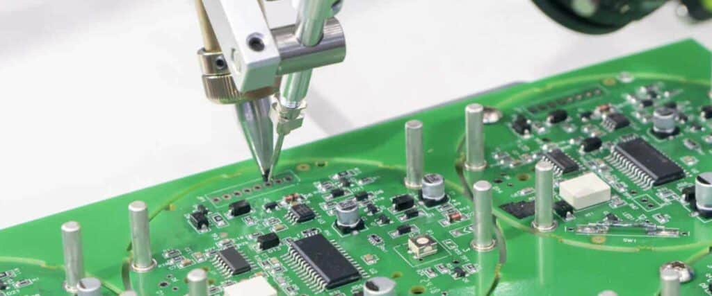
- First, check the PCB for any visible defects, such as solder bridges, cold solder joints, or misplaced components. Correct any issues found.
- Connect the input voltage source to the PCB and measure the output voltage using a multimeter. The output voltage should be approximately the same as the input voltage, minus the diode voltage drops.
- Use an oscilloscope to check the output waveform. The waveform should be a pulsating DC voltage with a frequency twice that of the input AC voltage.
- Load the circuit with a resistor and measure the output voltage again. The voltage should remain stable under load.
Troubleshooting
If the circuit does not function correctly during testing, some common issues may be the cause. Here are some steps to follow during troubleshooting.
- Check the diodes for proper orientation and functionality. A faulty diode can cause the circuit to malfunction.
- Check the PCB for any shorts or open circuits. Use a multimeter to test for continuity between the components.
- Verify that the input voltage is within the specified range for the circuit. An input voltage outside the specified range can cause the circuit to malfunction.
- Check the load resistor for proper value and functionality. An incorrect or faulty load resistor can cause the circuit to malfunction.
Overall, testing and troubleshooting are crucial steps in ensuring the proper functioning of a full wave bridge rectifier PCB. By following the steps outlined above, any issues can be identified and corrected, resulting in a functional and reliable circuit.

