A full wave bridge rectifier is an electronic circuit that converts alternating current (AC) into direct current (DC). It is commonly used in power supplies and other electronic devices that require a steady DC voltage. The circuit consists of four diodes arranged in a bridge configuration, which allows both halves of the AC waveform to be rectified.
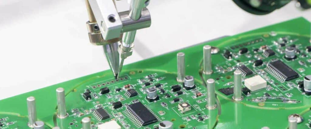
The layout of a full wave bridge rectifier printed circuit board (PCB) is crucial for its proper functioning. The PCB layout determines the placement of the components and the routing of the traces that connect them. A well-designed layout can minimize noise and interference, reduce voltage drop, and improve thermal performance. On the other hand, a poorly designed layout can lead to erratic behavior, overheating, and even damage to the components. Therefore, it is important to follow some guidelines and best practices when designing a full wave bridge rectifier PCB layout.

Overview
A full wave bridge rectifier is a circuit that converts alternating current (AC) to direct current (DC). It is commonly used in electronic devices and power supplies. The PCB layout of a full wave bridge rectifier is important for its proper functioning and reliability.
What is a Full Wave Bridge Rectifier?
A full wave bridge rectifier is a circuit that consists of four diodes arranged in a bridge configuration. It is used to convert AC to DC by allowing only the positive half-cycle of the AC waveform to pass through the circuit. The diodes in the circuit are arranged in such a way that they conduct in pairs, allowing the current to flow in one direction only. This results in a smoother DC output voltage compared to a half-wave rectifier.
Why is PCB Layout Important?
The PCB layout of a full wave bridge rectifier is important for several reasons. Firstly, it affects the overall performance and reliability of the circuit. A well-designed PCB layout can help reduce noise and interference, improve thermal management, and increase the lifespan of the components.
Secondly, the PCB layout affects the cost and complexity of the circuit. A poorly designed PCB layout can lead to increased manufacturing costs, longer production times, and a higher likelihood of errors during assembly.
In summary, the PCB layout of a full wave bridge rectifier is an important aspect of its design. It affects the performance, reliability, cost, and complexity of the circuit. A well-designed PCB layout can help ensure the proper functioning and longevity of the circuit.
Design Considerations

Component Selection
When designing a full wave bridge rectifier PCB layout, it is important to consider the selection of components. The diodes used in the rectifier circuit must have a voltage rating that is greater than the maximum expected input voltage. Additionally, the diodes must be capable of handling the maximum expected current without overheating or failing.
The smoothing capacitor used in the circuit must have a capacitance value that is appropriate for the expected load current and output voltage. If the capacitance value is too low, the output voltage may have excessive ripple. Conversely, if the capacitance value is too high, the circuit may take longer to reach the desired output voltage.
Sizing and Placement of Components
The size and placement of components in a full wave bridge rectifier PCB layout can have a significant impact on the performance of the circuit. The diodes and smoothing capacitor should be placed as close as possible to the rectifier bridge to minimize the length of the traces between them. This can help to reduce the resistance and inductance of the traces, which can lead to lower voltage drops and improved efficiency.
The size of the traces used in the PCB layout should be appropriate for the expected current. If the traces are too small, they may overheat and fail. Conversely, if the traces are too large, they may take up too much space on the PCB and increase the cost of manufacturing.
Heat Dissipation
Heat dissipation is an important consideration in any electronic circuit, and a full wave bridge rectifier is no exception. The diodes used in the rectifier circuit can generate significant amounts of heat, particularly if they are operating at high currents. To prevent overheating, it is important to provide adequate heat sinking for the diodes.
The smoothing capacitor can also generate heat, particularly if it is operating at high currents. To prevent overheating, it is important to select a capacitor with a low equivalent series resistance (ESR) and to provide adequate heat sinking.
In summary, when designing a full wave bridge rectifier PCB layout, it is important to carefully consider the selection, sizing, and placement of components, as well as heat dissipation. By paying close attention to these design considerations, it is possible to create a circuit that is efficient, reliable, and long-lasting.
PCB Layout Guidelines
When designing a Full Wave Bridge Rectifier PCB layout, there are several guidelines to follow to ensure that the circuit functions properly. The placement of components, routing of traces, grounding, and decoupling capacitors are all important factors to consider.
Placement of Components
The placement of components is crucial in ensuring that the circuit functions properly. The diodes, capacitors, and resistors should be placed as close to each other as possible to minimize the length of the traces. This reduces the parasitic inductance and capacitance, which can cause unwanted oscillations and noise.
Routing of Traces
The routing of traces is also important in reducing parasitic inductance and capacitance. The traces should be kept as short as possible and should be routed in a way that minimizes the loop area. This reduces the amount of noise that is introduced into the circuit.
Grounding
Grounding is an important consideration in any PCB layout. The ground plane should be kept as clean as possible, and the ground connections should be kept short and direct. This reduces the amount of noise that is introduced into the circuit and ensures that the circuit functions properly.
Decoupling Capacitors
Decoupling capacitors are used to filter out noise and ensure that the circuit functions properly. They should be placed as close to the power pins of the ICs as possible and should be connected directly to the ground plane. This reduces the amount of noise that is introduced into the circuit and ensures that the circuit functions properly.
In summary, when designing a Full Wave Bridge Rectifier PCB layout, it is important to consider the placement of components, routing of traces, grounding, and decoupling capacitors. By following these guidelines, you can ensure that your circuit functions properly and is free from noise and unwanted oscillations.
Testing and Troubleshooting
Testing the PCB
Once you have completed the PCB layout for your full wave bridge rectifier, it is important to test it to ensure that it is working correctly. Before you begin testing, make sure that you have all the necessary equipment, including a multimeter and a power supply.
To test the PCB, first connect the power supply to the input terminals and measure the output voltage using the multimeter. The output voltage should be equal to the input voltage minus the voltage drop across the diodes. If the output voltage is too low or too high, check the connections and components on the PCB.
Next, check the current flowing through the PCB using the multimeter. The current should be within the rated specifications of the components used on the PCB. If the current is too high, check for short circuits or incorrect component values.
Common Issues and Solutions
There are several common issues that can occur when testing a full wave bridge rectifier PCB. Here are some solutions to these issues:
- No output voltage: Check the connections and make sure that the diodes are properly oriented.
- Low output voltage: Check for loose connections or damaged components.
- High output voltage: Check for incorrect component values or a short circuit.
- Excessive heat: Check for incorrect component values or a short circuit.
In addition to these issues, it is important to ensure that the PCB is properly grounded and that there are no stray wires or components that could cause a short circuit.
By following these testing and troubleshooting steps, you can ensure that your full wave bridge rectifier PCB is working correctly and reliably.
