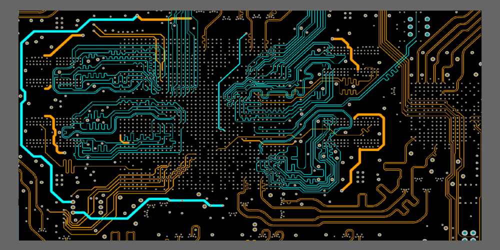
Rectifier PCB layout is an essential aspect of designing power supplies and other electronic circuits. The rectifier circuit converts AC voltage to DC voltage, and its proper functioning is crucial for the overall performance of the circuit. A well-designed rectifier PCB layout ensures that the circuit operates efficiently, with minimal noise and interference.
The layout of a rectifier PCB involves careful consideration of the placement of components, routing of traces, and grounding scheme. The placement of components should minimize the length of the traces connecting them to reduce parasitic inductance and capacitance. The routing of traces should also be optimized to minimize the loop area and reduce electromagnetic interference. Grounding is also crucial in a rectifier circuit, and proper grounding techniques should be used to ensure that the circuit operates reliably.
Basics of Rectifier PCB Layout
Single-Phase Rectifier Layout
When designing a PCB layout for a single-phase rectifier, there are a few important considerations to keep in mind. One of the most important is the placement of the rectifier diodes. These diodes should be placed as close as possible to the AC input terminals to minimize the length of the AC traces. This helps reduce the inductance of the AC circuit and improves the efficiency of the rectifier.
Another important consideration is the placement of the filter capacitor. This capacitor should be placed as close as possible to the rectifier diodes to minimize the length of the DC output traces. This helps reduce the inductance of the DC circuit and improves the stability of the output voltage.
Three-Phase Rectifier Layout
When designing a PCB layout for a three-phase rectifier, the layout is more complex than a single-phase rectifier. The rectifier diodes should be placed in a bridge configuration, with each diode connected to two of the three-phase inputs. The placement of the filter capacitor is also important, and it should be placed as close as possible to the rectifier diodes to minimize the length of the DC output traces.
In addition, it is important to ensure that the current is evenly distributed between the three phases. This can be achieved by using a star or delta connection for the three-phase inputs. A star connection is recommended for rectifiers with a low output current, while a delta connection is recommended for rectifiers with a high output current.
Overall, the PCB layout for a rectifier is an important consideration in the design process. By following these basic guidelines, designers can ensure that their rectifiers operate efficiently and reliably.
Factors to Consider in Rectifier PCB Layout
Heat Dissipation and Thermal Management
Heat dissipation and thermal management are critical factors to consider in rectifier PCB layout. The rectifier circuit generates a significant amount of heat, which can damage the components and reduce the circuit’s efficiency. Therefore, it is crucial to design the PCB layout in a way that facilitates heat dissipation and thermal management.
To achieve this, designers should consider using heat sinks, thermal vias, and copper pours. Heat sinks can be used to dissipate heat from high-power components such as diodes and transistors. Thermal vias can be used to transfer heat from one layer of the PCB to another, while copper pours can be used to increase the thermal conductivity of the PCB.
EMI and Noise Control
Another critical factor to consider in rectifier PCB layout is EMI and noise control. The rectifier circuit can generate electromagnetic interference (EMI) and noise, which can affect the performance of other components in the circuit and cause malfunctions.
To minimize EMI and noise, designers should consider using proper grounding techniques, shielding, and filtering. Grounding techniques such as star grounding can help reduce ground loops and minimize EMI. Shielding can be used to protect sensitive components from EMI, while filtering can be used to remove noise from the circuit.
Component Placement
Component placement is another critical factor to consider in rectifier PCB layout. The placement of components can affect the circuit’s performance, efficiency, and reliability. Therefore, it is essential to place components in a way that optimizes the circuit’s performance.
Designers should consider the placement of high-power components such as diodes and transistors, as well as the placement of passive components such as resistors and capacitors. Placing high-power components away from sensitive components can help reduce EMI and noise, while placing passive components close to the components they are filtering can improve their performance.
Trace Routing
Trace routing is the final critical factor to consider in rectifier PCB layout. The routing of traces can affect the circuit’s performance, efficiency, and reliability. Therefore, it is critical to design the PCB layout in a way that optimizes trace routing.
Designers should consider the length and width of traces, as well as the spacing between traces. Long and narrow traces can increase resistance and reduce efficiency, while short and wide traces can improve efficiency. Spacing between traces can affect EMI and noise, so designers should consider spacing based on the circuit’s requirements.
Design Techniques for Rectifier PCB Layout

Grounding Techniques
Grounding is one of the most critical aspects of rectifier PCB layout. It is essential to create a low impedance path for the return current to flow back to the power source. For this, it is recommended to use a star grounding technique, where all the ground connections converge at a single point. This technique helps to minimize the ground loop area and reduces noise and interference.
Component Selection and Placement
The selection and placement of components play a vital role in the performance of rectifier circuits. It is recommended to use high-quality components that can withstand high voltage and current. The placement of components should be done in a way that minimizes the length of the traces and reduces the parasitic inductance and capacitance.
Trace Width and Spacing
The trace width and spacing should be carefully chosen to handle the high current and voltage in rectifier circuits. It is recommended to use wider traces to minimize the resistance and voltage drop. The spacing between the traces should be sufficient to prevent arcing and breakdown of the dielectric material.
Copper Pour and Shielding
Copper pour and shielding can help to reduce noise and interference in rectifier circuits. Copper pour refers to the process of filling unused areas of the PCB with copper to create a solid ground plane. This technique helps to reduce the ground loop area and provides a low impedance path for the return current. Shielding refers to the use of a conductive material to isolate sensitive components from external noise and interference.
In summary, the design techniques for rectifier PCB layout include grounding techniques, component selection and placement, trace width and spacing, and copper pour and shielding. By following these techniques, it is possible to create a high-performance and reliable rectifier circuit.
Testing and Troubleshooting of Rectifier PCB Layout
Testing Techniques
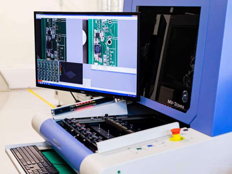
When testing a rectifier PCB layout, it is important to have a good understanding of the circuit and the expected output. One common technique is to use a multimeter to measure the voltage across the output terminals. The measured voltage should match the expected output voltage. It is also important to check for any abnormal heat or smell coming from the components, which could indicate a problem.
Another useful testing technique is to use an oscilloscope to measure the output waveform. The waveform should be smooth and free of any spikes or distortions. Any abnormalities in the waveform could indicate a problem with the layout.
Common Issues and Solutions
One common issue with rectifier PCB layouts is the presence of ripple voltage on the output. This can be caused by insufficient filtering or a faulty capacitor. To solve this problem, it is important to ensure that the correct value of capacitor is used and that it is connected properly.
Another common issue is overloading of the circuit, which can cause the components to overheat and fail. To avoid this, it is important to ensure that the circuit is designed to handle the expected load and that the components are rated appropriately.
In addition, incorrect component placement or wiring can cause problems with the rectifier PCB layout. To avoid this, it is important to double-check the circuit diagram and the physical layout of the components before assembling the PCB.
Overall, careful testing and troubleshooting can help ensure that the rectifier PCB layout is functioning properly and reliably. By using the appropriate testing techniques and addressing any common issues, it is possible to create a high-quality rectifier PCB layout that meets the desired specifications.
