Rapid advancement in the field of electronics leads to the end of the era of long GPS navigators. These days you don’t have to depend on big navigators to guide you in directions as your ancestors did ages ago. Regardless of this aging technique of navigating GPS, it is much easier to integrate GPS into PCBs.
A device with a Printed Circuit Board GPS antenna has never been confirmed to be taken directly. However, regardless of your experience in GPS or RF design, you can focus on creating a PCB with GPS capabilities. Before diving into the details of the manufacturing process, let’s look into what is the GPS-printed circuit board.
What GPS PCB Board Entails?
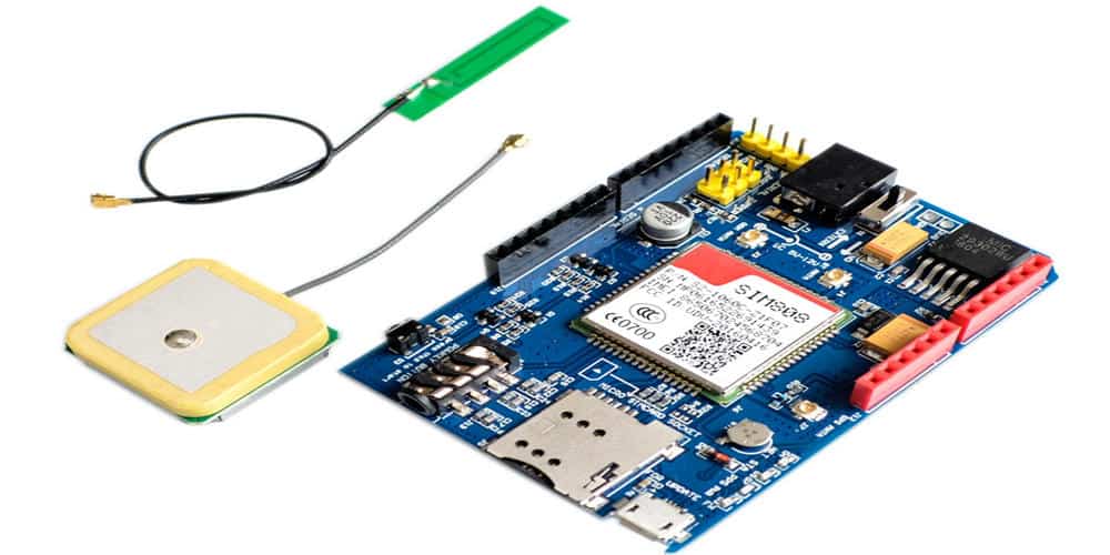
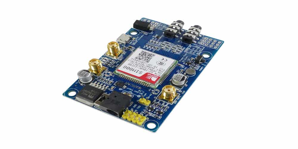
A GPS PCB mainly requires a small circuit board integrated with a GPS navigator device. GPS navigator device contains a GPS patch antenna, a GNSS antenna, and a ceramic patch. While designing GPS PCB, make sure to focus on the area of both the GPS antenna and PCB. The area for the planned application also plays a vital role in the manufacturing process. However, the GPS antenna is one of the crucial aspects of GPS PCB as it ensures the types to a large context.
Active & passive GPS PCB Board Antenna
There are two types of GPS PCB antennae, active and passive antennae. The main difference between active and passive antennae is that one is integrated with a low-voice amplifier while the latter lacks it. Active antennae are directly placed on the board and connected to it with the help of a copper cable.
Both types come with prepackaged receivers. Moreover, there is also a passive connecting network that enables 50 Ohms output of a pattern of potential radiation. Furthermore, the active antenna has a much better performance advantage due to its LAN. LAN controls the noise amount during the output signal, while the noise often leads to a higher sensitivity.
As a passive antenna has no LNA, that’s why it needs one on the circuit board to control the quality of the signal as it travels through a low-voice amplifier from the receiver. Any unnecessary noise can make it more vulnerable and sensitive as LNA is solely designed to decrease the noise of output signals. Furthermore, while choosing an external receiver for LNA, make sure that the signal that goes through LNA must be protected from external EMI or crosstalk as much as you can so that you get a better result.
GPS Antenna in Circuit Board Design

It’s important to understand that encompassing GPS antennas into PCBs turn them into a source of intermixed signals. Each signal’s noise from the crosstalk or EMI raised at the point of the input antenna lessens the quality of the signal. Moreover, it might also completely block the signals of the antenna rather than making it tolerable to the noise of the ground plane. It mostly occurs when it is not sufficiently integrated from components around.
Another important thing to note is that all other components presented on PCB need to be isolated properly. If not, then there is a chance that the antenna and receiver might lessen the strength of the signal. In most cases, the receiver proves to be the worst source to lower the signals, especially when it has an engraved antenna. Furthermore, apart from isolation crosstalk, the receiver between the other components needs proper shielding.
Filtering is also important for filtering the signals of GPS. One proven way of accomplishing this filtration is by putting a SAW filter between Low Noise Amplifier and the receiver. A surface acoustic wave(SAW) filter allows filtration of high frequency (more than 1GHz). It is available in GPS applications.
Grounding & Routing
The GPS output signal from the antenna and GPS receiver often ranges around 30dB, which is under the noise surface. Such the lowest noise is often acceptable but could cause blockage of the GPS receiver’s signal. This would help the GPS device to function properly while having a complete process – routing, shielding, and grounding.
In most scenarios, turning primary PCBs into well-functioned blocks also suggests that each comes with its own ground planes. Later, the planes are then routed back again to the initial ground state to prevent any ground loops. Therefore, there are a variety of conditions to follow whenever the size of the ground plane is concerned. As in small devices like mobile and gadgets, the size of ground planes encircles a GPS receiver which makes it difficult to follow the requirements.
However, connecting the RF and ground planes is possible by shielding the receiver, external signal LNA and its connecting network within a shielding can. The only thing that is important to be noted here is to integrate the ground plane from the GPS receiver along with its matching networking. Later connect it with the ground plane at one specific point. The most appropriate area to degrade the clock and data line is the RF ground plane.
Antenna traces of GPS that pass through the receiver convey analog signals. These signals are put down far away from the PCB components and traces. If feasible, then circulate the antenna traces within the shielded space. However, it is most likely possible to ground the traces of the antenna within the internal PCB ground rather than ground planes of matching circuits on both sides. Ensure that the implanted antenna should be placed outside the ground of the shield so that you can easily protect the components and battery from the antenna.
Factors to Consider in Choosing GPS PCB Board
Today, GPS modules and chipsets have become an essential source for many industries and consumer devices. The increasing demand for GPS emphasizes the fact that it is a vital need of every designer and engineer. It is understandable as they are responsible for incorporating GPS in their devices and gadgets and PCBs.
However, the noted fact is that not every PCB designer is well-known and experienced in the field of GPS PCB designs. Therefore, it is more resourceful to follow the design pattern to manufacture a successful GPS PCB.
Considerations
First of all, choose the desired GPS module or chipset for the PCB as it would be helpful further in choosing GPS solution plans and also how to integrate them further.
Conclusion
Recently, GPS-printed Circuit boards have become the essential source of navigating the land, air, and sea. Understanding knowledge of its design and importance helps you to design better. Hopefully, this article helped you thoroughly to understand how GPS PCB is designed and why it is important in today’s electronic industry.
