As there is advancement in technology, then our gadgets become smaller. As they reduce and become smaller, to function, they need small circuit boards. There is nothing like standard circuit boards. The design for each of the boards out there, serves a specific purpose and a specific item.
PCBs come with many defined requirements, and expert manufacturing and an engineering team is required to transform your concepts into something real or test an already-existing prototype, ensuring that it meets the tolerance needs. However, if something comes out of spec, there are many engineered solutions, which can help in solving your issues and still keep you on a budget.
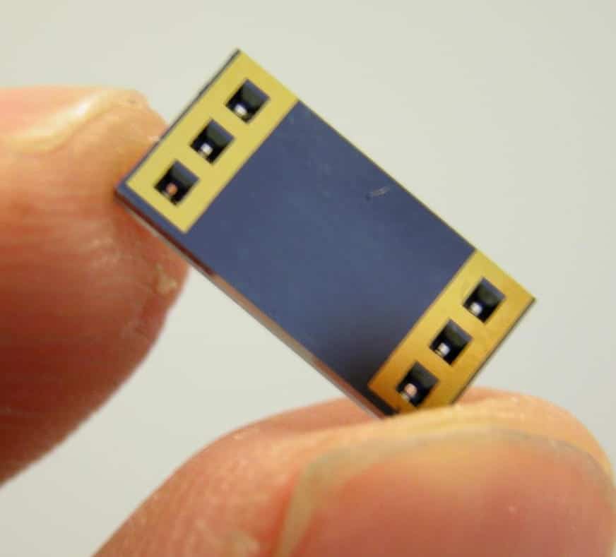
In this article, we will reveal how useful small circuit boards are in today’s technology world.
Circuit Boards Necessary for Small Applications
Your board’s size has a lot to do with your design. In creating the layout of the circuit, you can make use of design software that is computer aided. With this, you can reduce your board’s size with ease. Most times, the spaces found in-between two paths that are electrical conducting are usually 0.006 inches or smaller.
Printed circuit board dimensions are usually based on its circuitry and the enclosure housing the printed circuit board. Also, it helps in determining the circuit’s fixed components and heat sinks. Using the software, the board’s size can be reduced easily. You may reach out to the Circuit board manufacturer to help determine what size they will produce.
The printed circuit board size also has to do with the enclosure’s available space. To design a small gadget, there is a need to utilize a small circuit board. However, note that when creating a design for your small bare PCB, it has to come with small components too. This could mean soldering these components using a soldering iron with a fine tip, as well as a close-up glass or a microscope, most especially when the holes have clearances that are tight.
Tips for Making Small PCB
To design your circuit, there are some factors you should look into. These include minimum width of the trace, minimum width of the silkscreen, size of the text, SMT solder mask width (minimum), minimum clearance of the solder mask, minimum space for the vias/pads/trace, and the finish and drilling hole. These factors help in determining the circuit board’s minimum size.
Check the buried and blind vias with care
Always take a look at the buried and blind vias with care. This is because they can impact your design significantly, and can help engineer your printed circuit board to become very small. Vias helps in connecting the traces between the layers of your board, and the traditional alternatives will reduce the routing space available on the boards.
Maximize the Routing Space
To maximize the routing space and prevent a larger size for the board, we advise that you consider some alternatives. Blind vias help in connecting the internal and external layers with little spacing. With buried vias, you will be able to connect many internal layers. However, they will not extend to the external layer. With this, there is a limit on the space requirement, which can deliver a product that is more stable.
Spacing in-between the components
Another thing you should look into is the spacing present in-between the components. When you bring them too close to each other, there may be no room left for the traces’ routing. The more the number of pins found in the component, the more space it will require. With appropriate spacing, soldering the components onto the circuit board becomes easier.
Also, components have to work with the general standard numbering design of the pin. This is to make sure that the orientation of everything is done equally. This reduces the possibility of mistakes all through the period of soldering and inspections. This helps in limiting the concerns of manufacturing, while assisting you to take note of everything while reducing the size.
Width lines that are larger will consume more space. However, this reduces your PCB heat with respect to dissipation.
Applications of Small Circuit Boards
As electronic gadgets continue to miniature, this has led PCBs to become denser and smaller, therefore requiring more capabilities. Today, small circuit boards are taking over, as many manufacturers prefer using integrated circuit chips. Small printed circuit boards are useful in the applications below.
- Instrumentation
- Power electronics
- Industrial use
- Semiconductor
- Contract manufacturing
- LED
Manufacturing Process of Small PCB Board

The resistance of electrical current across the surface of printed circuit boards via copper network is necessary. All the parts of smallest circuit boards come with some complicated copper routes
Consistent Design for Small PCB Output
The designer’s configuration of a small PCB making use of a program must be perfect for the small PCB board. It is advisable that designers advise the maker of their project about the modem firmware for the design of the circuit, before they go ahead with producing the printed circuit board. This prevents problems that could result due to inconsistencies. Softwares that are useful in designing the circuit board include Eagle, OrCAD, Pads, KiCad, etc.
After the authorization of all the specifications of the PCB board, the design is then exported to assist their producers. Extended Gerber is widely regarded as the most frequently used program. At times, it is also referred to as IX274X.
The birth of the Gerber in the printed circuit board industry came as the perfect performance format. Different software for PCB designs of small batches includes different measures in order to create Gerber files, as well as other significant details such as openings, box drawing, components’ notations, and layers for copper tracking.
Here, all the aspects of PCB manufacturing should undergo tests. This program conducts the algorithms design checking to ensure that there are no defects. Frequently, designers review their plans for edge spacing, hole size, and track distance features.
Manufacturing the Rings of Small PCBs
After the output and the designers, then it is time for the printing of the PCB to begin. Here, manufacturers conduct DFM inspections. They utilize the printer called Flatbed scanner for printing the smallest circuit boards. It also permits picture films on these boards.
Manufacturers always make use of these films to snap the PCB board. The output reveals an acrylic layer having a black pigment photograph of printed circuit boards. The picture’s all-visible part reveals the area of the non-conductive substance.
The external parts make use of the opposite way, which is transparent for the copper. The contriver manufactures this film in a gradual process, keeping your file safe from any unwanted interaction.
For each layer of the solder mask and PCB, it gets a black and transparent film sheet. PCBs with double layers require about four sheets. Tow sheets will be for the layers, while the remaining two will be useful as solder cover. Also, all the films have to match each other perfectly.
To make sure that there is perfect synchronization for all the films, you have to register them using registration troughs. You can achieve the hole precision by the manipulation of the table, where the film lies on. If the table’s small size leads to a perfect match, then the hole becomes stung.
Printing of the image on the copper foil
To produce small-batch pubs, you can prepare the individual printed circuit board. The basic PCB type is composed of laminated boards having a glass or epoxy fiber called substrates. The laminate is the perfect reception body for the copper, which forms your narrow printed circuit board. Furthermore, its substratum material offers the oriented circuit board with a dustproof and robust base. In the end, the pre-bonding of the copper takes place. The method deals with getting rid of the copper. This exposes the template of the film.
To build your small pcb, cleanliness is very important. The laminate preset on the side with copper is moved to a decontaminated setting after washing. At this point, there must be no dust particles settled on it. With a spot of dirt, the circuit becomes accessible or short. Also, the clean panel then gets a film layer that is photosensitive referred to as resistant photography.
Join the layers perfectly
This is where you get your small circuit board right. You must join your small pcb board properly and then get the layers set for testing. Next, you have to connect the solid rock with the outermost layers. This device is finalized in two major stages, which includes layering up and bonding.
Furthermore, the layering for the external part is composed of fiberglass sheets that are pre-saturated using epoxy mastic. Another name for the shorthand is prepreg.
Drilling
Here, you bore holes into your stacking board. The two components are intended for use later on like copper links through leaded aspects and troughs, relied on the precise boxes’ accuracy. You bore the cavity to a hair breadth, with the boiler having 101 microns as its diameter, as well as the hair measuring 152 microns.
In identifying the box targets’ precision, there’s an x-ray locator, which helps in detecting the right targets of the box. You then bore the correct registration holes to ensure that more holes are secured.
Deposition of Copper and Plating
After you drill, the panel shifts further into the board. This phase fuses the different layers using chemical deposition. This small PCB board is then subjected to some chemical reaction sequences after some serious washing. Next, the copper bonds over the board’s surface, which has a thickness of about 1 micron.
Final Etching
Here, unwanted copper layers are removed. This is done by adding some chemical solutions. During this stage, the remaining copper gets some protection from the tin.
Application of solder mask
This next stage requires cleaning the boards, and then coating it using an ink. After this, you can apply the solder mask on the frame’s edges. The boards are then made to pass through UV light that passes via a photographic sheet. The protected part stays unhardened and then it is taken out.
Protect using chemical cover
This stage requires you to protect your small PCB board with chemical cover, using either silver or gold. This gives your small circuit board extra solder capacity. All through this process, the pads of some printed circuit boards overheat, which results in uniform mats.
Electrical Testing
This stage, an expert takes the small circuit board and goes on to carry out an electrical test. This is to help in judging the measure of the final product. This gives the reliability of the printed circuit board.
Benefits of Small Circuit Boards
Below are some of the benefits of small circuit boards
Saves space
Small circuit boards are great for small devices. For these small devices, the manufacturer fits the circuit board, as well as other components.
Cost reduction
With miniaturization, the materials required for the manufacturing of the device is reduced. The use of less materials leads to cost reduction, helping you save some money. One benefit you are sure to get from here is lower transportation cost. You will be able to transport much smaller products at a reduced fee. Also, you don’t have to spend more when creating a small circuit board compared to other board types.
Efficient
Smallest PCBs are usually efficient. They provide great dissipation. This is why they are useful for consumer electronics. Asides from this, these boards come with great electrical, as well as thermal properties.
Environmentally friendly
You need just a few materials for producing a small printed circuit board. This is why the process is environmentally friendly. Using fewer materials will yield less waste.
Conclusion
It is clear that the smallest circuit boards offer lots of great benefits. The boards are useful for producing smaller devices. This is why they play a great role in the electronic industry of today. Although small printed circuit boards have a small size, fabricating them could be a complex process. This is why manufacturers must pay special attention when fabricating this type of circuit board.
