PCB Design Process
The initial step involved when it comes to designing a PCB board is to create the schematics. This is done with software that’s tailored for making printed circuit boards. It can be used with various other programs to achieve this. These are some that have been highlighted below as you read through the other sections of this article.
This is a summary of the processes involved:
Use the component library and draw the circuit diagram. This means that the circuit arrangement for the PCB boards will be changed for the best possible fit.
When a circuit is finished, you can then create it in a plastic box. Gerber’s files can be printed as masks or negatives on plastic sheets. This enables you to select the correct substrate for the intended circuit. There are several options to choose from, such as; unbroke glass or fiber sheets, etc.
What is a printed circuit board?
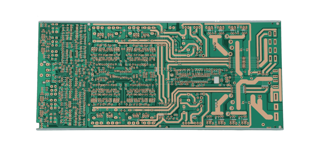
Do you use old electronics like the television remote? If you have and have seen its insides exposed, then you’ve most likely seen a PCB. There are many green sheets in the world that feature that silver threaded board with patterned components. The sheet is purely a computer board.
PCBs form a foundation for many complex circuit boards and are a major reason for having smaller screen sizes. It consists of electronic components with electrical connections made with copper traces. These are made in two or multiple layers according to the complexity of the circuitry.
PCB: Terminologies
As we start our way through the development process for Printed Circuit boards, let’s go through some of the common words in the glossary. Once the basics of the concept and design of the PCB have been explained, you will need to find out the types of PCB available. Having a basic knowledge of this can be helpful to you when it comes to choosing a suitable circuit or getting your own circuit boards.
Multilayer PCB
Multilayer PCB refers to PCBs that have at least 2 layers of conductivity. The PCBs are usually viewed as two-part conductive sheets that are laminated and then glued together with the second dielectric sheet. The manufacturing procedure can be tedious.
As more layers increase, copper sheets are kept thick to avoid bulking the circuit board. As layers are added to PCBs, they result in powerful and dense assemblies. This is what prompted a fast multilayer PCB. It can then connect via shunt to each layer using electrical wires.
Rigid-Flex PCB
The PC board consists of two layers, rigid as well as flexible. Since flexible PCBs lack strength, combining the layers with rigid layers gives the PCB the allowance to form rigid structures. This product is made of single-layer, double-layer, or multilayer PCBs. Because of its space-efficient design, it’s an ideal choice for a medical electronic circuit such as a pacemaker and is also a suitable circuit for aerospace phones, etc.
Single Layer PCB
As the name suggests, this type of layer, single-layer PCB type contains just one layer of conductive material like copper sheets. A solder mask protects the conductive sheets before being screened by the silk screen. you can easily identify The single Layer Printed Circuit Board by its marked or traced sides. It has been used for very simple circuiting such as camera circuits, toy circuits, radios or stereo sets, etc.
Flexible PCBs
Flexible PCBs or CFPCBs in general are easy to bend. The device saves space and is smaller than the stiff PCB. It is mainly made from materials such as polyamide, PEEK, or transparent polypropylene. Because it is easy to produce, this PCB is available in single, double, and multilayer applications including LCD manufacturing, Flex solar panel, and smartwatch.
Throughhole PCB
As its names indicate the component is connected by a lead wire that goes over the PCB holes in the form of an integrated circuit. The method is easily implemented on an isolated PC board. As the layers are increasing the difficulty of implementing them increases. Despite its limited use, this technique is currently in steep decline.
Double Layer PCB
Double layers are composed of two layers of conducting materials. Non-conductive materials like plastic and glass are glued together between copper sheets. This is a common PCB type used as a medium for complicated applications. Then there’s the close route trace feature, which is unlike the single-sided PCBs.
Rigid PCB
It is essentially rigid and abates PCBs from twisting and turning. A common substrate for rigid PCBs is FR4(with a stiffening agent). Once the PCB is assembled, it won’t have to fold. It is sturdy with optimum durability and hence a great choice for computer motherboards.
Surface Mount PCB
Its newer technologies eliminate the drill hole for connecting SMD parts. This component is mounted directly onto the PCB. This is very easily realized no matter what layer the board contains.
Common PCB Layout and Design Software
W can’t say that there is a universal standard when it comes to printed circuit boards. With the wide range of possibilities that exist, it is quite easy for a novice to get overwhelmed. This list includes PCB designing software below, and we would be identifying two popular ones, although other alternatives to them that are also available.
Free PCB Basic Design Software for Beginners

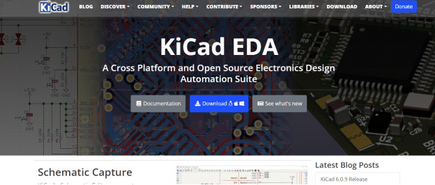
KiCad – It’s the perfect choice when you are introducing yourself to PCB design basics. It provides free software for creating PCB layouts and schematic designs and has an interactive 3D viewer.
Professional PCB design software

Altium Designer – This is a widely used PCB design software, Altium, and it provides an impressive array of features with a reasonable price that matches.
Basics of Starting a New PCB Design
PCB design is a standard workflow that requires an understanding of the process. PCB design is a typical process where an engineer’s design is finished and the final design for the production is drafted.
Design rules are key to success
Once you understand the production process and some of the basic capabilities of PCB manufacturers, it’s easier to understand the limitations that design rules have. The main DFM problem that is often encountered is the size of copper features on the PCBs or the separation of the different features.
The default rules on PCB design are normally conservative and you’ll know if your design rules are broken. For example, a footprint that is sized from pad-to-pad at approximately 9m can trigger an error in an architectural design rule that occurs when a component is copied onto a PCB structure.
Use ground planes
Each PCB must have a ground connection so that every component of the design can form completing circuits and so that the supply of electricity continues through the entire construction of all the components. Grounding can come via the battery on the motherboard or via another power source.
No matter what is connected, the ground connection is needed for the rest of the PCB. By far, the easiest way is to use a ground plane in which a layer in this PCB can be ground using copper sheets covering all the surface area. I am still amazed that countless designers have hesitated to put a ground plane into their computer chips.
Sometimes, because the device doesn’t have a ground plane, many fundamental noise issues that often affect both analog and digital signals can be identified. The use of a stable ground plane across your device is a good practice for contemporary printed circuit boards (PCBs). In certain cases, the use of star ground or split planes on the PCB is acceptable, but they are not suitable for the greater majority of analog and digital designs.
Learn about the PCB manufacturing process
Basic knowledge about the design of physical products is that they should be manufactured at scale. The software can easily integrate design features into the layouts of PCBs and other products. Your design decisions must be made in standardized procedures therefore the designer must be acquainted with the limitations of the fabricated components in a PCB. All PCB designers should learn at least the basic techniques in PCB manufacturing.
This will allow the complete manufacturing and quality control of designs. Those practices must be integrated into your design process called Design for Manufacturing (DFM).
Complete placement before routing
Once you have transferred CAD data to new PCBs, it’s important to place the component parts around them. The goal here is to put together the components for the solution of the design and ensure it flows easily. Therefore you should not do a routine until all the necessary information is received to ensure a complete component placement.
In case you have a route without any component placement, it will always require changing the PCB routing. Ensure your layout is arranged so that net crosses are reduced. After everything has been put together, and you have a complete component placement, the final step will begin the PCB insertion.
Schematics and Layouts must be synchronized
Depending on how you plan to get started, designing your PCBs will likely need some of these. If you change your layout, it must be synchronized across the schematics on the layout. This may also include the following design changes:
Once changes occur the modifications must be applied to the PCB layout. It’ll happen using your computer’s import feature. When all of your designs are now fully synchronized with the design engines of your software, then they can now read all the design data accurately in the system.
Understand the PCB Design Workflow
It is good to take a few minutes to get acquainted with the basic workflow. The design workflow is outlined in the following list.
PCB: Classification
Print circuit boards can be grouped according to design usage and other factors. Below is an example of the various classifications of printed electronics.
Type of PCB based on their flexibility
Some printed circuit boards can be divided into three kinds based on how flexible they are. The substrate being employed is the only thing it depends on.
PCB design software
Here is a list of some common PCB design software you can test. You can find the best tools in PCB design & layout for learning some of these popular applications.

Autodesk Eagle
One of the best schematic platforms is Autodesk Eagle, formerly titled CadSOFT Eagle. Autodesk Eagle has added many helpful functions to its platform. These include the layout editors, PCB layout editor to design PCB components and routing of the circuit boards. It is supported by many operating systems like Linux, Windows, and macOS.
KiCAD
Founded in 2003, KiCad was created as an open-source electronic design automation solution across several platforms. It comes with 3D schematics views allowing the creation and editing of designs from 32 copper sheets.

Altium Designer
In addition, Altium provides 3D visualization directly through the PCB editor. The software is useful in developing schematics of medium to complicated circuits.
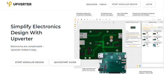
Upverter
Because it uses an open-source hardware design format, Upverter is among the web-based collaboration Electronic design automation (EDA) platforms. Among its many features are a 3D view, simple hardware export, PCB editor, and schematic capture.
Osmond
Osmond PCB provides a powerful resolution of ten nanometers, giving a high-precision output, and is specifically designed for Mac users. You may edit traces and re-structure the integrated circuits at any time using the tools provided, and it offers flexible features like limitless board sizes, support for both the imperial and metric unit systems, and much more.
The designs are based on their flexibility and it determines their uses. PCs in the standard PCB category are grouped according to their flexible characteristics:
What are the basic steps of PCB design?
Guide to design for PCBs.
- Know the electrical properties.
- Making a diagram.
- Use software for the creation and analysis of schematics on a PCB design.
- Make a stack of the PC boards.
- Set out the design criteria.
- Place all the pieces together.
- Place the drillings there.
Routers
- Understand electrical parameters.
- Making a diagram
- Make an easy-access schematic capture system.
- Create an electronic circuit board stacker
- Specify design guidelines.
- Put the parts together
- Inject drill hole.
- Send copper traces.
FAQs
What is a PCB basic?
Printed circuit boards (PCBs) refer to mechanical boards with tracks and footprints that reflect the design schematics. Modern PCBs are constructed on nonconductive substrates topped by copper layers.
What is the first step in PCB design?
The Schematics are the first phase of the circuit board design Process Schema. It represents the logical representation of electronics on the circuit board to be built, using industry standards and it is used to illustrate various component parts.
What are the three basic methods to make PCB?
The basic ways of making a computer are by using iron on Glossy paper, Circuits by hand in PCBs, and Laser engraving.
