Table of Contents
ToggleGSM PCB antenna reference design is a critical aspect of wireless communication. Antennas are essential components of any wireless system, and their design is crucial to the performance of the system. A well-designed antenna can improve the quality of the signal and increase the range of the wireless system.
The design of a GSM PCB antenna requires careful consideration of several factors, including the frequency range, radiation pattern, and impedance matching. The antenna’s frequency range must match that of the wireless system to ensure optimal performance. The radiation pattern of the antenna determines the direction and strength of the signal, while the impedance matching ensures that the antenna can efficiently transfer power to the wireless system.
In this article, we will explore the key considerations involved in designing a GSM PCB antenna reference design. We will discuss the various types of antennas available and their advantages and disadvantages. We will also look at the design process, including simulation and testing, to ensure that the antenna meets the required specifications. By the end of this article, readers will have a better understanding of the critical role that antenna design plays in wireless communication.

Design Requirements
Frequency Band
The first design requirement for a GSM PCB antenna is to select the frequency band of operation. GSM operates in various frequency bands, including 900 MHz, 1800 MHz, and 1900 MHz. The antenna design must be optimized to operate within the selected frequency band. The frequency band selection is critical in determining the antenna’s physical size, gain, and radiation pattern.
Impedance Matching
The second design requirement for a GSM PCB antenna is impedance matching. The antenna must be impedance-matched to the feed line to avoid signal reflection and ensure maximum power transfer. Impedance matching is achieved by selecting the appropriate antenna dimensions and feed point location. The antenna’s input impedance must match the characteristic impedance of the feed line, typically 50 Ohms.
Radiation Pattern
The third design requirement for a GSM PCB antenna is the radiation pattern. The antenna’s radiation pattern must be optimized to provide sufficient coverage in the desired direction. The radiation pattern is influenced by the antenna’s geometry and feed point location. The antenna’s radiation pattern must be consistent across the frequency band of operation.
In summary, the design requirements for a GSM PCB antenna include selecting the frequency band of operation, impedance matching, and optimizing the radiation pattern. The antenna’s physical dimensions, feed point location, and geometry are critical in achieving the desired performance.
Antenna Selection

When designing a GSM PCB antenna, selecting the right antenna is critical. The antenna’s performance and efficiency are directly related to the overall system’s performance. In this section, we will discuss the types of antennas and their placement.
Types of Antennas
There are several types of antennas suitable for GSM PCB designs. The most common types include:
-
Monopole Antennas: These are the most common type of antenna used in GSM PCB designs. They are easy to integrate and have a small form factor. They are suitable for use in small devices such as smartphones and wearables.
-
Patch Antennas: These are another popular type of antenna used in GSM PCB designs. They are thin, lightweight, and have a low profile. They are suitable for use in devices with limited space.
-
Helical Antennas: These antennas are suitable for use in devices that require a high gain. They are often used in GSM modems and routers.
Antenna Placement
The placement of the antenna is also critical to its performance. The following factors should be considered when placing the antenna:
-
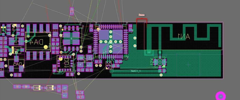
Ground Plane: The antenna should be placed on a ground plane for optimal performance. The ground plane should be at least 1/4 wavelength in size.
-
Clearance: The antenna should be placed away from other components to avoid interference.
-
Orientation: The antenna should be oriented in the correct direction for optimal performance. The orientation can affect the gain and radiation pattern.
In conclusion, selecting the right antenna and placing it correctly is critical to the performance of a GSM PCB design. By considering the factors discussed in this section, you can ensure that your design has optimal antenna performance.
PCB Layout

Trace Width and Spacing
When designing a GSM PCB antenna, the trace width and spacing are important factors to consider. The trace width should be wide enough to handle the current flowing through it, but not so wide that it takes up too much space on the PCB. The spacing between the traces should be sufficient to prevent any interference between them.
There are various online calculators available to help determine the appropriate trace width and spacing for a given application. It is important to keep in mind that these calculations are only a starting point and may need to be adjusted based on the specific design requirements.
Ground Plane
The ground plane is an essential part of the GSM PCB antenna design. It provides a low impedance path for the return current, which helps to reduce interference and improve the antenna’s performance. The ground plane should be as large as possible, covering the entire area beneath the antenna.
It is also important to ensure that the ground plane is continuous and free of any gaps or breaks. Any discontinuities in the ground plane can lead to unwanted radiation and reduced antenna efficiency.
Feed Line
The feed line is the connection between the antenna and the transmitter or receiver. It should be designed to minimize losses and impedance mismatches. The feed line should be as short as possible, with a low impedance throughout its length.
One way to achieve a low impedance feed line is to use a microstrip or stripline configuration. This involves placing the feed line on a separate layer of the PCB, with a ground plane above and below it. This configuration helps to reduce losses and improve the impedance match.
In summary, the PCB layout is a critical aspect of designing a GSM PCB antenna. The trace width and spacing, ground plane, and feed line all play important roles in the antenna’s performance. By carefully considering these factors and using appropriate design techniques, it is possible to create a high-performance GSM PCB antenna.
Simulation and Testing

Simulation Tools
Simulation tools play a crucial role in the design of GSM PCB antennas. They allow designers to predict the performance of their antennas before they are fabricated. This saves time and money and helps ensure that the final product meets the required specifications.
One popular simulation tool for GSM PCB antennas is CST Microwave Studio. This software allows designers to simulate the behavior of their antenna in a variety of scenarios, such as different frequencies, polarization, and angles of incidence. It also provides a range of visualization tools to help designers understand the behavior of their antenna.
Another popular simulation tool is Ansys HFSS. This software is similar to CST Microwave Studio and provides many of the same features. However, it also includes a range of advanced features, such as the ability to simulate the effects of environmental factors like rain, snow, and fog.
Testing Equipment
Testing is an essential part of the design process for GSM PCB antennas. It allows designers to verify that their antenna meets the required specifications and to identify any issues that need to be addressed.
One common testing method is the use of an anechoic chamber. This is a room designed to eliminate reflections and other sources of interference. It allows designers to measure the performance of their antenna in a controlled environment.
Another testing method is the use of a network analyzer. This is a piece of equipment that measures the electrical properties of the antenna, such as impedance and return loss. It allows designers to verify that their antenna is operating as expected and to identify any issues that need to be addressed.
In conclusion, simulation and testing are essential parts of the design process for GSM PCB antennas. By using simulation tools and testing equipment, designers can ensure that their antenna meets the required specifications and performs as expected.
Optimization Techniques
Tuning Components
One of the primary optimization techniques for a GSM PCB antenna reference design is to tune the components of the antenna. This involves adjusting the length and width of the radiating element and the ground plane to achieve the desired resonant frequency and impedance matching.
The tuning process can be done using a network analyzer, which can provide valuable information about the antenna’s performance. By adjusting the antenna’s dimensions and measuring its response, the designer can fine-tune the antenna to achieve optimal performance.
Matching Network
Another optimization technique for a GSM PCB antenna reference design is to use a matching network. This network is used to match the antenna’s impedance to the impedance of the transmitter or receiver.
The matching network can be implemented using various components, such as capacitors, inductors, and resistors. The designer needs to select the appropriate components and adjust their values to achieve the desired matching.
It’s important to note that the matching network can also affect the antenna’s radiation pattern and efficiency. Therefore, the designer needs to carefully consider the trade-offs between impedance matching and antenna performance.
In summary, optimizing a GSM PCB antenna reference design involves tuning the antenna’s components and using a matching network to achieve optimal performance. By carefully adjusting the antenna’s dimensions and selecting the appropriate components for the matching network, the designer can ensure that the antenna meets the desired specifications.
Conclusion

In conclusion, designing a GSM PCB antenna can be a challenging task, but with the right knowledge and tools, it can be achieved successfully. This reference design provides a good starting point for those looking to design their own GSM PCB antenna.
One of the key takeaways from this reference design is the importance of understanding the requirements of the GSM system and the antenna’s performance parameters. By carefully selecting the antenna’s dimensions and optimizing its layout, it is possible to achieve good performance and reliable communication.
Another important aspect to consider is the choice of materials and manufacturing techniques. The use of high-quality materials and precise manufacturing processes can significantly improve the antenna’s performance and durability.
Overall, this reference design provides a solid foundation for designing a GSM PCB antenna. By following the guidelines and recommendations outlined in this article, designers can create a high-quality antenna that meets the requirements of the GSM system and provides reliable communication.

