PCBs are the driving force for the ever-evolving electronics industry. The Fabrication process could be challenging and fascinating, but the transformation process has not stopped. The PCB design size has changed over time. The industry modified the size from a big size to a smaller compact size.
The design detail of the PCB forms an integral aspect of delivering a perfect functional PCB. Therefore, adequate attention is necessary for every process step as required. There are varying types of PCBs to meet the actual purpose of their designs.
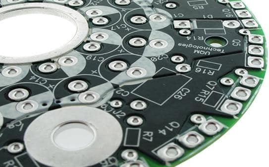
High current PCBs are in systems with high power applications. Applications that operate on high currents have some unique challenges. These difficulties are not associated with smaller digital applications. High current PCBs do not have a specific definition.
High current PCB design could only mean a board with high current components. They produce currents that are beyond the standard Amps. A high current PCB could be open to challenges that might lead to design failure. To ensure a perfect circuit operation, vital precautions are non-negotiable.
Thermal management and power supply are some of the essential factors for consideration. Furthermore, this article will explore some salient points that need scrutiny. Also, it will discuss processes that reduce risks associated with high current PCBs.
——————————————————————————————————————
Request High Current PCB Quote , Pls Send Files to Sales@raypcb.com Now
——————————————————————————————————————
High Current PCB Design Layout Essentials
Designing a high-current PCB requires different procedures against fabricating a low power design.. Components might face a reduced life span due to their exposure to high temperatures. Also traces affected by excessive heat could break. Exposing the power supply to an explosion due to short-circuiting could also be a setback.
High Current PCBs are at the risk of overheating and electric shock due to direct current. Therefore the board layout should come first in the early stage of the PCB design. High current PCBs operate on a rule that determines the path by which the power flows on the board.
The amount of heat a PCB needs to dissipate depends on the amount of power that moves through the circuit. The factors that influence the layout of high current PCBs are as follows:
- Materials used for the production of the PCB
- The Power level moving through the circuit.
- The thickness of the elements that occupy the board
- The volume of airflow affecting the board
- The environmental temperature of the location the board operates from.
To produce an efficient, and safe high current PCB, enacting these principles is vital.
Thermal Management
Designing PCBs with different components needs the inclusion of the thermal management system. This is to enable each component on the circuit board to keep safe temperature limits. The temperature on the board should not exceed the limit stated in the producer’s datasheet. Therefore, the connection pins move the heat generated by each element out of the board.
As the industry evolves, modern electronic elements producers design thermo-compatible packages. This has complicated heat dissipation on the board. Thus, to improve PCB thermal management, there are two major techniques used. They are:
- Thermal Vias insertion
- Creation of larger ground planes
Thermal Vias Insertion: This is the technique used to transfer heat from one layer to another layer on a single board. The thermal vias move heat from the hottest points on the board to other layers.
Creation of large ground planes: This technique enables the creation of extra space on the PCB for heat dissipation. Most times, planes connected to the upper or lower layer of the board are for extended heat exchange. The inner layers of the board could also serve as an extracting tool for heat dissipation.
Numerous components used in electronic circuits are highly sensitive to fluctuations. Detecting thermal differences could alter the signal produced. It could also generate errors that would reduce the reliability of the device.
These sensitive elements should be thermally insulated. The insulation protects the circuit board from the influence of heat.
Components Placement
The position of high current components on the PCB is a very crucial step required in its design. They are the components that generate the highest volume of heat on the board. Components like power transistors and voltage converters should not occupy spaces near the edges of the board.
These components generate heat build-up that raises the temperature on the board significantly. To allow heat diffusion on the board, combined elements should occupy the center of the board. This also enhances reduced temperature across the board.
It is crucial to note that the cluster of high current components is not advisable in the same area of the board. This is to put off the formation of heat spots on the circuit board. A setting that allows the mixture of high and low current components is preferable.
Components placement should begin with the power elements. Their traces should maintain a very short distance and enough wideness. This would help remove noise generation and ground loops. Generally, the following rules govern component placement.
- High current circuits should maintain a far distance from sensitive circuits.
- Identification and reduction of current loops within high current paths
- Adequate grounding measures for the board
- Reduction of resistive voltage drops
Furthermore, components could be better placed on different boards. This is possible provided the form factor allows it on the device.
Materials
Designing high current PCBs requires the usage of unique materials with special features. Thermal conductivity is the first feature required. It is a material component that suits high current PCB design. This feature helps reduce heat temperature where it is high.
Conductive and thermal materials with the same thermal expansion coefficient are features. In the absence of these features, the materials would face expansion or contraction. This is due to their exposure to high temperatures. Thus, the thermal and conductive materials help minimize mechanical stress on the materials.
Solder Mask
Removal of the solder mask enables the trace to carry a larger amount of current out the board. This technique enables the PCB trace to stand against excessive heat. The trace width does not need any increase to perform the task. Though, copper materials augment extra solder to increase copper thickness that fights heat.
The Significance of Via Current Calculations
Vias have resistance and inductance capacity. Routing a trace from a side of the PCB to another requires low inductance or resistance. The size of the via needs consideration due to the resistance value it possesses. Larger vias possess low resistant strength. This affirms their usefulness for high current nodes and grounding filter capacitors.
Via could also affect the current flow in the PCB. Resistance in vias could lead to loss of energy in the form of heat dissipation. Thus, the after-effect could be harmful to the functionality of the PCB. Calculating the current carrying capacity of vias is very crucial. It will enhance the acceptability of the high current PCB design.
Calculating the via current could involve complex parameters. However, all is not off track as accuracy is the benchmark for the modern business world. Thus, calculations needed for high current PCB designs are no pushovers. The IPC- 2152 standard enjoys universal acceptance for via current calculations.
IPC -2152 standard on PCB Via Current Calculator
To design a PCB, knowing the current carrying capacity of the board is crucial. The conductors on the PCBs are the conveying elements. It is important to learn what the via current capacity is. The focal point for high current PCB design is the trace and via current carrying capacity
Its main aim is to keep the temperatures on the conductors below the required limit. This will help the components maintain cool temperatures on the board. IPC 2152 has the agreed current carrying capacity of Vias for the electronic industry.
The IPC is the trade association for the electronic industry. They supply the standards for the protection and assembly of all electronics equipment. IPC standards are well recognized and most acceptable in the electronics industry.
IPC-2152 offers PCB producers the ability to keep the proper functionality of PCBs. The Via current calculator computes the current via needed as temperature standard. IPC- 2125 – This standard supplies the via current-carrying capacity limits.
Furthermore, Via possesses other properties that need consideration. They include Via Voltage drop, Via impedance, Via direct current resistance, Via Capacitance, Via thermal resistance, Via inductance, Via resonant frequency, and Via power dissipation in dBm.
IPC-2152 standard examines the distance between traces and copper planes on the board. It also provides results for thermal conductivity, vias, and board materials. This is about the trace and current. Thus, the online calculator is an invaluable tool. It calculates the correct trace and current capacity for a set temperature rise.
The IPC-2152 standard offers easily accessible data. Its efficiency increases the design and quality of the PCBs. Via current calculation forms an essential part of the PCB design.
——————————————————————————————————————
Request High Current PCB Quote , Pls Send Files to Sales@raypcb.com Now
——————————————————————————————————————
Routing PCBs through Microvia
PCBs are at the center of electronic products. They supply a corridor that links all electronic components to enable functionality. PCBs design could be a single layer or multilayer design. To establish connections on the multilayer PCBs, the producer fixes the layers together.
Furthermore, electrical connections between layers go through drilled holes on the PCB. The holes are copper plated, also referred to as plated through-holes or Vias. The holes could be microvia depending on the diameter.
IPC defines microvia as any drilled hole with an aspect ratio of 1:1 that does not go beyond a 0.010-inch depth. It was previously considered based on size, provided it is equal to 0.006-inch depth or smaller. To avoid changing the definition, IPC maintained the aspect ratio of 1:1 as its standard.
Microvia could also mean a smaller type of normal via. Though it has a structure that differs a little, and it is cone-shaped. The microvia reaches a single layer to maximize its reliability strength. Fabricators can use stacked microvias to set up connections over multiple layers.
Microvia also called uVias plays the connecting role between layers on the circuit board. However, it does not connect more than two layers in a circle. Microvia current capacity is very low due to its resistance level. It could safely carry 2amps of current.
Features of Microvia
There are different types of microvias, but they have two common features.
Low Aspect Ratio
As opposed to through-hole vias in normal PCBs, microvias possess a small aspect ratio. Their aspect ratio is ideally 0:75-1. A larger ratio of 1:1 or much more to 2:1 if fabricated brings reliability doubts. Due to their small aspect ratio, microvias span best between a single-layer.
Please note that any aspect ratio beyond 1 does not align with the IPC definition of a Mircrovia.
Proneness to Fracture at the Neck
Microvias are prone to breakage at the neck area when placed under strong vibration. The fracture could also occur when under repeated thermal cycling or mechanical shock. This fragility is due to the plating methods used. Copper curved into the barrel area will lead to stress concentration. It weakens the neck area.
Types of Microvia
The Microvia has different types drilled on the PCB. Each of the hole sizes maintains an equal aspect ratio of 1:1. However, their placements on the board vary.
The Blind Microvia: It enables connections from the surface to the inner layer of the PCB. The drilled hole is from a side of the board not like the through-hole. It does not go through the entirety of the PCB
Staggered Microvia: This type of microvia allows balanced placement on one another. Many buried microvias connect the layers when placed on each other.
Via-in-Pad Microvia: It implies placing microvia holes on the copper solder pad of the components. It is a technique that enables miniaturized PCBs.
Stacked Microvia: This via type allows for many buried or blind microvias piled on each other. It will enable connections of the inner layers.
Conclusion
High Current PCB designs allow for flexibility in its fabrication process. The IPC standards will guide manufacturers to design reliable devices. When selecting components and materials for design, the IPC standards have the approved materials for all the processes.
