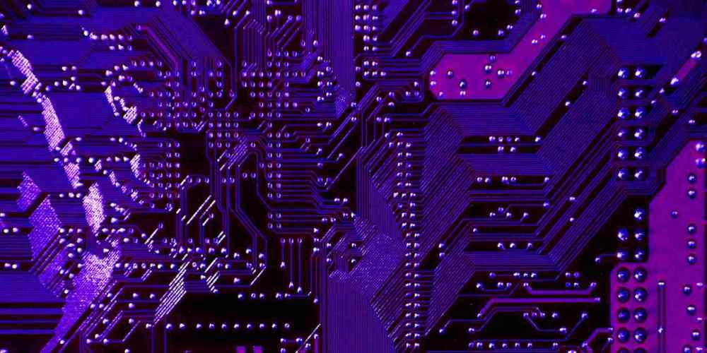
Circuit boards need more power or current, as the demands of the applications or devices increase. If you must use one of these boards, you have to be sure that it matches the devices’ operating requirements. The use of the high current PCBs became imperative, owing to the ever-increasing demand for circuits that can be used for higher applications.
This article covers everything you need to know about the high current PCB design.
Why is a PCB said to be “High Current?”
When a Printed Circuit Board (PCB) is so-called, it simply means that the “current densities” it uses are higher than those used by traditional circuit boards. It is also said to be “high current” due to the provision of stronger connection points.
You can also be sure that this type of PCB can handle higher rates of electrical current, while resisting the higher temperatures for a longer time.
The Safety Precautions
While it is safe to say that this type of circuit board handles huge current flows better, it can also be said that it does that in line with the safety demands.
Due to the designation for use with high-powered devices, it is common to find the high current PCB used as an interface between these devices and the safety measures meant to be in place.
The systems and devices that operate with more power tend to expose the users to more dangers, ranging from electrostatic discharge and unsafe operating conditions. With the high current PCB, one can mitigate some of these challenges, due to the fact that the circuit can handle such currents.
The Difference between High Current PCB & Heavy Copper PCB
The two are often interchanged and sometimes, seen to be one and the same. However, a tiny line of difference separates them.
On the one hand, we have the high current circuits, being the circuit boards that carry thousands of amps, support higher current densities than the traditional PCBs do, while resisting higher temperatures for an extended period.
On the other hand, the heavy copper PCBs are the ones that have up to 3 oz of copper, and which has a thickness of up to 4 oz per ft2.
The closest affinity between the high current PCB and the heavy copper PCB is that the former possesses a thicker and a heavier layer of copper, which bolsters the circuit’s durability.
The Processes to Designing the High Current PCBs
Now, let us go into the details on how best you can start making your first and subsequent designs for the circuit boards using higher currents.
1. Stick to Using Thicker Boards
You may think that using a thinner or tinier board can make the difference, especially when you consider the greater conduction it offers away from the other components.
However, when you note that the copper is heavier and the typical applications are for more power usage, opting for the thicker PCB becomes a better option.
These reasons should encourage you to choose thicker PCBs over thinner one for high current circuit designs:
- Greater Mechanical Support: this type of board is perfect for circuits that use heavier components. You can count on this to improve the mechanical capabilities of the large heatsinks, as well as support the board-mounted inductive components.
- Heavy Copper is the Best: it is a common standard for the traditional circuit boards to have between 17.5 microns and 1 oz per square foot as the thickness. However, you can be sure that this is not sufficient when working with the high current PCB. Direct Current (DC) power loss is commonly created when there is a resistance of the copper used in the traces. Therefore, opting for heavier copper does not only prevent DC losses, but also takes less space due to the reduction of the trace width.
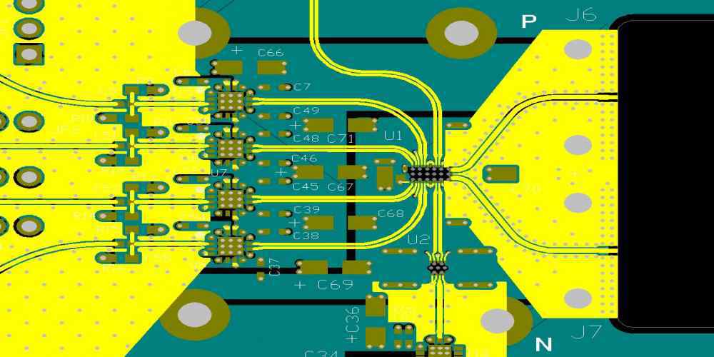
2. Reduce the Trace’s Length

The longer the trace is, the higher the chances that it becomes a threat to the power flow. Due to the increased resistance, it becomes obvious that the lengthened trace, especially the one that carries current, could negate power supply.
However, if you can use shorter traces, you can be certain that it would not only reduce power loss, but also retain more of it.
3. Replace the Traces with Power Planes
Both traces and power planes could improve the flow of power, depending on the length. However, it may be a better option to replace the trace and use the power planes instead.
The reason for this is that the power planes could help accommodate more of the needs, without having to take up much space.
4. Employ the Use of Polygon Pours
Due to the higher applications’ requirements, you may find out that the high current PCB doesn’t meet up with up to 70% of those requirements, especially as they relate to the current-carrying capacity.
If that be the case, it is a good opportunity to consider employing the use of “polygon pours.” What are those, you may ask? Polygon pours are used not only to increase the circuit’s current-carrying capacity, but to also make a thermal isolation of the sensitive components.
The process to using these is to pour or place the polygon pours under the chip and having them connected to the PCB via a vias.
5. You Don’t Need the Solder Mask
It may interest you to know that the use of solder mask in a high current PCB could be negating the goal of the PCB, which is to facilitate current transfer. Instead, the solder mask would reduce the amounts of current being carried due to the coverage of the copper underneath the board.
Through the solder mask removal, this copper is not only exposed, but is also supplemented with additional solder. This helps to decrease the overall resistance in the current-carrying parts of the PCB, while increase the copper’s thickness.
6. Use Copper Bars for Higher Current Supply
If you don’t want to try the other methods, perhaps, using copper bars would give you the desired results.
These are solderable copper bus bars that can be attached to the PCB’s pads via soldering. The aim is to transfer a bulk of the higher currents to these bars.
Would these copper bars be able to handle the currents? Yes, they could and that is because of the higher thickness than what traces could offer. With this increased thickness comes higher current-carrying capacities, while retaining almost the same width.
7. The Sensitive Components Should be Thermally-Isolated
The challenges peculiar to the high current PCB design are not limited to getting around the current-carrying capacities. They also have a lot to do with how the components react under these higher current densities.
The rule of thumb is to isolate or separate the sensitive components from the rest of the board. By sensitive components, we mean those PCB parts that are prone to malfunctioning, after getting exposed to certain environments and conditions. Examples include converters, voltage references, amplifiers and regulators.
By separating or thermally-isolating these components, you help to protect them from having altered signals, as well as reducing the chances of opening up the circuit board to errors.
8. Use the Proper Grounding Strategies
Ideally, a Ground (GND) in a Printed Circuit Board (PCB) is not meant to be separated or split up. However, exceptions are made for PCBs requiring either higher voltages or higher currents, as is the case now.
The exceptions made here include the separation of the Ground (GND) between the following:
- Regulated DC sections
- Unregulated DC sections and;
- The input AC
The following are other important points to note about the ground-splitting:
- Isolated Strategy Usage: this entails the earthing of the input side and the disconnection of the output side from the Ground (GND).
- 3-Wire DC Arrangement: an arrangement of three (3) Direct Current (DC) wires can also be made. These wires are GND, PWR and COM. The earth connection is usually made with the GND wire.
9. Ensure an Effective Heat Dissipation with Thermal Vias and Landings
The high current PCB, due to the increased heat generation, needs to have a suitable means of dissipating or getting rid of some of the heat.
The best practice is to use a combination of thermal vias and thermal landings. On the one hand, the thermal vias are used for a wide range of purposes, including directing the flow of heat from the circuit and utilizing the basic conduction capability to absorb the heat produced by the higher current that passes through the circuit board.
The thermal vias works this way for the high current PCB:
- Heat absorption
- Transfer of the heat to the thermal vias
- The transportation or transfer of the heat energy to the thermal landings.
The thermal landing is a metal plate located at the PCB’s bottom. It works by protecting the important circuit components from the negative impacts of high power, while ensuring that there are no failure points in the process. It is also to this thermal landing that the heat will be transferred.
10. Use Via Stitching to Improve Current Transfer
Commonly, a trace needs to be routed or connected to an additional layer if it is unable to carry the required current through a single layer.
When this is the case, a via stitching needs to be done between the two layers. Doing this helps to current-carrying capacity, especially if the two traces on the different layers use the same width.
11. Maintain an Excellent Electronic Component Placement
It is imperative to have the electronic components appropriately placed, mounted or positioned atop the PCB’s surface. That is a sure way to bolster the flow of currents on the board.
These tips should help you:
- Avoid Heat Accumulation: heat or thermal energy begins to accumulate on the board when the components that produce an increased amount of energy are not evenly-spaced. Ideally, these parts should not be placed close to the PCB’s edge, as that is where they tend to accumulate more heat and significantly heat up the board’s temperature.
- Component Distribution: just as you are trying to avoid placing the components at the edge, it is also important to space them. The best spacing option is to distribute these parts to different parts of the board. This way, they wouldn’t be united to produce more heat in one place.
- Microcontroller Positioning: the Microcontroller (MCU) is best mounted at the center of the circuit board. This does not only reduce the PCB’s temperature, but also dissipates heat effectively across the board.
12. Internal Layers Can be Used for High Current Connections
It is wrong to think that only the outer or external layers can be used for high current PCB design. The internal layers can also come in handy, most especially, when there is limited or no space on the exterior layers.
What you will do in this case is to make a solid fill-in an internal layer, followed by connecting it to the higher current devices on the outer layers, using vias.
Final Words: The Components Make all the Difference
Above all, you may be unable to get the most out of your high current circuit board if the components do not work accordingly. It will interest you to know that the components have a major role to play, primarily because they generate much of the heat/current and mainly because they will be impacted by the current on the board.
Choosing the right components can help you improve the reliability of the PCB. As much as you are going for the ones with higher current capacities, you also want to dig deeper to make a better choice.
Some of the factors worth considering are the thermal resistance values, as well as the current ratings – that is, if you are working with the inductive components and MOSFETs.
No matter the type of components you choose to use or the design iteration you opt for, choosing Hillman Curtis is a major step to getting your high current PCB designed the right way. We help bring your ideas to life and offer professional guidance every step of the way.
