In the world of electronics, IR sensors are becoming increasingly popular. These sensors are used to detect the presence of objects or people by emitting infrared radiation. However, the effectiveness of an IR sensor depends on the quality of its printed circuit board (PCB) layout.
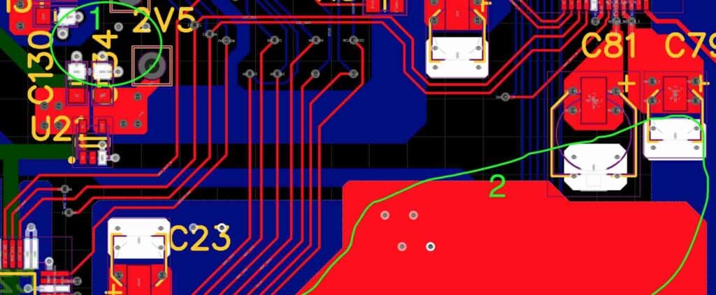
The PCB layout of an IR sensor is critical to its performance. The layout must be designed to minimize noise and interference, while maximizing the sensitivity of the sensor. This requires careful consideration of the placement of components, the routing of traces, and the grounding scheme. A well-designed PCB layout can improve the accuracy and reliability of an IR sensor, making it an essential component in a wide range of applications, from security systems to industrial automation.
Designing an IR sensor PCB layout requires a deep understanding of electronics and circuit board design. It is not a task to be taken lightly, as even small mistakes can have significant consequences. However, with the right knowledge and tools, it is possible to create a high-quality PCB layout that will ensure the optimal performance of an IR sensor.
IR Sensor PCB Layout Basics
When it comes to designing an IR sensor PCB layout, there are a few key considerations to keep in mind. In this section, we’ll cover the basics of IR sensor PCB layout, including sensor placement, signal traces, and ground plane.
Sensor Placement
The placement of the IR sensor on the PCB is critical to its performance. The sensor should be placed in a location where it will have an unobstructed view of the target area. This means that the sensor should be placed near the edge of the PCB, with no components or traces blocking its view.
Signal Traces
The signal traces for the IR sensor should be kept as short as possible to minimize the chance of noise and interference. The traces should be routed away from other high-speed signals and power traces to reduce the risk of crosstalk and interference.
Ground Plane
A solid ground plane is essential for the proper operation of the IR sensor. The ground plane should be placed on the opposite side of the PCB from the sensor to minimize interference. The ground plane should be connected to the PCB ground using multiple vias to ensure a low impedance connection.
In summary, when designing an IR sensor PCB layout, it’s important to consider the placement of the sensor, the routing of the signal traces, and the placement of the ground plane. By following these basic guidelines, you can ensure that your IR sensor PCB layout will perform optimally.
Designing for Optimal Performance

Sensor Sensitivity
When designing an IR sensor PCB layout, it is important to consider sensor sensitivity. This involves choosing the right components and layout to ensure that the sensor can detect the intended signals accurately. One way to achieve this is by selecting a sensor with high sensitivity and a low noise floor. Additionally, proper placement of the sensor and its components can help reduce interference and improve sensitivity.
Noise Reduction
Noise is a common problem in IR sensor circuits. It can come from a variety of sources, including power supplies, electromagnetic interference (EMI), and thermal noise. To reduce noise, it is important to use proper grounding techniques and shielding. This can include placing the sensor and its components as far away as possible from sources of noise, using shielding materials, and minimizing the length of signal traces.
Filtering Techniques
Filtering is another important aspect of designing an IR sensor PCB layout. It can help reduce noise and improve signal quality. There are several types of filters that can be used, including low-pass filters, high-pass filters, and band-pass filters. The choice of filter will depend on the specific requirements of the application. It is also important to consider the cutoff frequency and the order of the filter when selecting components.
In summary, designing an IR sensor PCB layout for optimal performance involves considering sensor sensitivity, noise reduction, and filtering techniques. By selecting the right components and layout, it is possible to achieve accurate and reliable detection of IR signals.
Manufacturing Considerations
When it comes to manufacturing an IR sensor PCB, there are several important considerations to keep in mind. These include PCB material selection, trace width and spacing, solder mask, and silkscreen.
PCB Material Selection
Choosing the right PCB material is critical for ensuring proper IR sensor function. The most common materials used for IR sensor PCBs are FR-4 and Rogers materials. FR-4 is a standard material that is widely used due to its low cost and good electrical properties. Rogers materials, on the other hand, are more expensive but offer superior electrical performance, making them ideal for high-frequency applications.
Trace Width and Spacing
The trace width and spacing of an IR sensor PCB are also important considerations. The width of the traces should be large enough to handle the required current without causing excessive heat buildup, but not so large that they take up too much space on the board. The spacing between the traces should be wide enough to prevent interference, but not so wide that it causes signal degradation.
Solder Mask
The solder mask is a protective layer that is applied to the PCB to prevent solder from flowing onto the wrong parts of the board. When designing an IR sensor PCB, it is important to ensure that the solder mask is applied only to the areas where solder is needed. This will help to prevent any interference with the IR sensor.
Silkscreen
The silkscreen is a layer of ink that is printed onto the PCB to label the various components and connectors. When designing an IR sensor PCB, it is important to ensure that the silkscreen does not cover any of the critical components or connectors. This will help to prevent any interference with the IR sensor.
In conclusion, when designing an IR sensor PCB, it is important to consider the PCB material selection, trace width and spacing, solder mask, and silkscreen. By keeping these considerations in mind, you can ensure that your IR sensor PCB functions properly and reliably.
