The LM3886 is among the widely accepted audio chip amplifiers. It has a firm place in the DIY sector. There are different factors that make it compelling for usage. These are a lower degree of distortion and fewer counterparts, and it is cost-efficient as well. It is important to select an appropriate layout and counterparts for these chips so that all these factors can come together to produce a remarkable audio amplifier that would be unmatched in terms of performance and budget.
Things To Keep In Mind Before Designing An Lm3886 PCB
There are some crucial parameters to keep in mind before producing an audio amplifier. The main factor is output power. Its needs to be decided prior to the entire setup of production of this chip. The average output of an power amplifier board ranges between 60-68 watts. Now, this can be variable on the basis of the desired output. Some other factors to pay heed to are impedance and voltage. Different speakers have variable impedance levels.
It is always available in the user manual for ease. There is also a need for specific input voltage for the entire production. It is the factor that your audio chip amplifier will work on to amplify it as its output. There are different mobile applications that analyze and set all of these parameters. It is better to work according to the AC voltage between different channels of this audio chip with the help of a special tool called a multimeter.
Determining The Required Power For Lm3886 PCB
The next step is to set the power supply voltage and power. Again, these parameters are different for all types of speakers. These are also helpful in evaluating the accurate VA score of the transformer in the audio chip.
This will generate the necessary power for its smooth working. Generally, transformers have less voltage, and the power of the amplifier will also be less due to the presence of this transformer in terms of output. In case when VA score of the transformer is below average, then it will create a negative impact on the audio chip by disrupting the audio when the volume is raised by the user.
Lm3886 PCB – Audio Amplifier Power Supply Voltage
It is important to evaluate the peak output voltage of the amplifier you are working on. The next step will be working on the power supply voltage.
Designing The Lm3886 PCB Ground Layout

The base layout of the amplifier under development is directly connected to the output of the amplifier. It is important for a layout to be flawless so that it can execute different functions. Number one is that the amplifier will deliver a silent output in case the when speakers are off. When the ground layouts are defective, then these will produce a considerate hum sound even when there is no music playing.
There is a proper guideline to rectify the issues with ground layouts. The current on the ground level should be less and must be away from the ground with a higher degree of current. The grounds with low currents are linkable with the input circuit system and loops. High current grounds are with the power supply capacitors, speakers, and Zobel network. The pathway of the current from high to low grounds is important. It produces a DC offset voltage and enhances the sound by amplifying it naturally. There is a viable method to keep a distance between high and low current grounds. Let’s discuss it below:
- Audio input ground means audio input cable for the ground
- The signal ground includes the input circuitry – Rin, Cc, and Ri/Ci
- Speaker ground is for the speakers
- Power ground defines a separate ground for main factors like the capacitors, Zobel network, and also the ground pin
Problems occur when the abovementioned grounds make frequent contacts with the main system ground. The main ground is positioned closer to the capacitors that act as reservoirs on the power supply path. The function of the main ground is to interlink the earth wire through a special circuit called a loop protection circuit and also with the amplifier chassis.
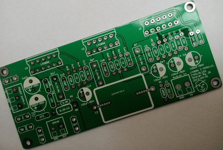
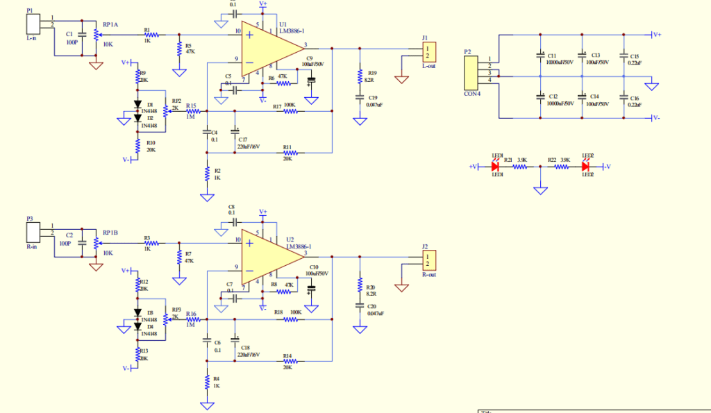
Designing The Lm3886 PCB Board
The designs of printed circuit boards determine the final performance of an amplifier. We are going to elaborate on the process of developing a fine layout of printed circuit boards. There are two circuits essential to produce an amplifier.
One of the remarkable tools in this pursuit is EasyEDA. It is a complete package to produce such designs and layouts. LM3886 PCB offers schematic drawings of these circuits. It is a free tool and can also handle custom-based production of printed circuit boards.
Ordering Circuit Boards
There is a button called “Fabrication Output” in this special PCB tool. It takes the users to a separate page that helps them order the desired circuit boards. There are different options available to select from the thickness of the copper, the overall size of the printed circuit board, the color of the circuit, and amount of items (circuit boards).
Lm3886 Printed Circuit Board Design Guidelines
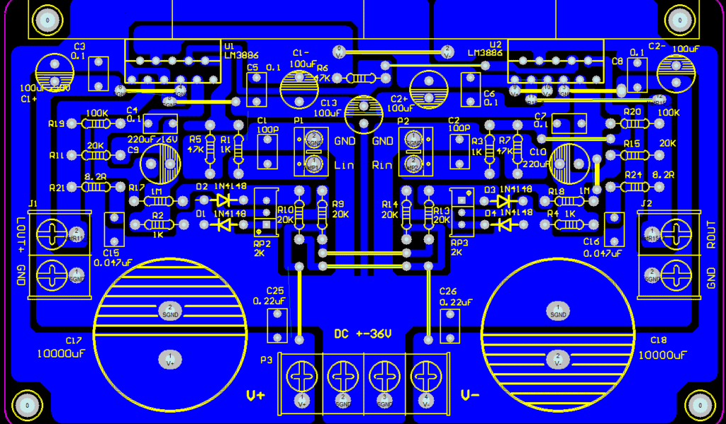
It is better to follow the instructions to produce good-quality circuit boards in order to produce amplifiers. The magnetic field is developable through the high level of current that flows through and makes its path between the power supply voltage. This magnetic field is important for producing a current in the loop and also in the input traces.
· There should be a right-angle distance between these two boards for proper functioning. This distance is helpful in the smooth routing of the circuit. Also helps in reducing the distortion as much as possible. These should also be on the contrary sides of the terminals so that it makes the routing easier.
· Any gap left develops an extra loop that receives the transmission and disturbs the electromagnetic field produced.
· The traces that are connected to the power supply and power ground should both be placed and routed in a close periphery so that there will be lesser odds of producing another loop. In the same way, the signal traces and audio input work their best when they are placed nearer.
· When ground planes are positioned on the lower layer of the printed circuit board, then it also reduces the chances of producing an extra loop that can disrupt this whole process.
· The ground network for printed circuit boards only predicates signal ground and power ground. There is a dedicated ground plane for each of these grounds. There is a high current in the power ground and a low current in the signal ground. These are at a considerable distance till both grounds come in contact with the main ground system.
· The Zobel network, power supply, and output are present on the upper layer of the circuit board. Their routing takes place on the ground plane as per the guidelines.
· The signal ground plane includes loops and input of the circuit board. Due to this reason, there is a large gap between the traces to handle the power supply so that there will be less inductance and resistance from the entire circuitry.
· The issue that comes with the inductive loads is that it opposes the smooth current flow and generates resonance when teamed up with the series capacitors. It also boosts the trace length, which is not essential for this specific pursuit.
· It is important to keep all the traces short in length to avoid these problems.
· The same is the case with other factors like loops, Zobel network, and input. One method to keep the traces short is to position all these circuit parts opposite to the pins of the audio chip.
Wiring Circuit Board All Together
We use all those audio chip amplifier components that are befitting for this purpose. The channel used for its product range from $100-$118 in total. The price is not for the amplifier chassis, wiring, and power supply constituents.
The amplifier is producible in a much more affordable range. It is important to adjust the corresponding footprints of these parts in the design to further process things in a feasible manner.
Solder Paste And Soldering for PCB layout
There is an important step to execute before proceeding to the soldering. A piece of sandpaper is useful for oxidation removal from the circuit parts for assembling. The benefit of this sub-step is to develop a stealthy joint in the soldering process that enhances electrical conductivity.
A puffy fabric is crucial to use to position and carry the circuit components during the soldering procedure. All of this happens on the upper surface of the circuit. It is essential to solder the smaller circuit parts before the larger ones.
The quality of eutectic solder is way better than regular tin-lead solder. It gives more margin for melting. It also develops another cold solder joint if any of the circuit parts dislocate from their original position. The benefits of using this solder are more electrical connectivity and fast setting.
Chassis Finding
There is a special space to keep the circuit parts secure and intact to not damage them during any process. The wires and all the connectors need a particular container-like structure so that these protect the amplifier from interruption from the radios and lights. There is a problem that occurs when it comes to finding a chassis that is befitting for the type of circuit.
How Does Lm3886 PCB Audio Amplifier Sound?
We are experts in producing premium-quality amplifiers that offer impressive performance. The bass of this amplifier is completely clear. The highs offered by our amplifiers are also smooth in working. Our amplifiers exceed the expectations of a reliable amplifier that serves longer for customers.
