Low noise PCB design is an important consideration for many electronic devices. It involves designing printed circuit boards that minimize the amount of electrical noise generated by the circuitry. This is particularly important for sensitive applications such as medical equipment, audio amplifiers, and scientific instruments.
The goal of low noise PCB design is to minimize the amount of electromagnetic interference (EMI) generated by the circuitry. EMI can cause a variety of problems, including reduced signal quality, increased noise, and even interference with other nearby electronic devices. By minimizing EMI, low noise PCB design can improve the overall performance and reliability of electronic devices. This is achieved through careful component placement, routing, and grounding, as well as the use of specialized components such as low-noise amplifiers and filters.
Benefits of Low Noise PCB Design
Reduced Signal Interference
Low noise PCB design reduces the amount of interference that can affect signals. This is because noise can be generated by various sources such as the power supply, components, and traces on the PCB. With a low noise design, the noise is reduced, and the signal is less likely to be distorted or lost.
One way to reduce interference is to use proper grounding techniques. This involves connecting all the ground points on the PCB together and ensuring that the ground plane is uninterrupted. This helps to reduce the amount of noise that is generated by the components.
Another way to reduce interference is to use shielding. Shielding involves placing a conductive material around the component or trace to prevent electromagnetic interference. This technique is particularly useful when dealing with high-frequency signals.
Improved Signal Quality
Low noise PCB design can also improve the quality of the signal. This is because noise can cause distortion in the signal, resulting in errors and reduced performance. By reducing the noise, the signal can be more accurate and reliable.
One way to improve signal quality is to use low-noise components. These components are designed to generate less noise, resulting in a cleaner signal. Another way to improve signal quality is to use proper trace routing. This involves ensuring that the traces are as short as possible and are not placed too close to each other. This helps to reduce crosstalk and other types of interference.
In conclusion, low noise PCB design can provide several benefits, including reduced signal interference and improved signal quality. By using proper grounding techniques, shielding, low-noise components, and proper trace routing, the noise can be reduced, resulting in a cleaner and more reliable signal.
Key Considerations for Low Noise PCB Design

When designing a PCB for low noise applications, there are several key considerations that must be taken into account. These include component placement, grounding and shielding, and trace routing.
Component Placement
The placement of components on a PCB can have a significant impact on the level of noise that is present. To minimize noise, it is important to keep high-speed digital components away from sensitive analog components. This can be achieved by physically separating the two types of components on the board.
Additionally, it is important to consider the orientation of components. For example, placing a resistor perpendicular to a trace can create unwanted noise. By placing the resistor parallel to the trace, the noise can be minimized.
Grounding and Shielding
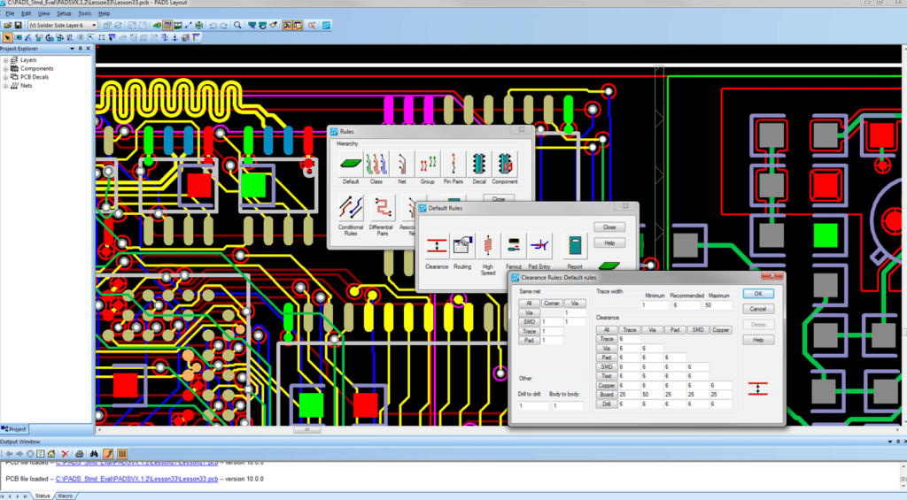
Proper grounding and shielding are critical to reducing noise in a PCB design. Ground planes should be used wherever possible to provide a low-impedance reference for signals. It is also important to ensure that all components are properly grounded.
Shielding can be used to protect sensitive components from external sources of noise. This can be achieved by placing a shield around the component or by using a grounded trace to create a shield.
Trace Routing
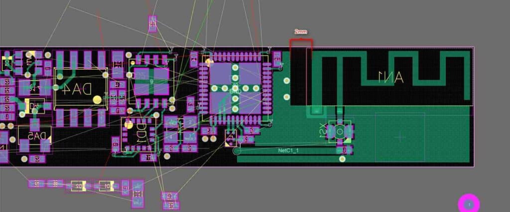
The routing of traces on a PCB can also have an impact on the level of noise present. To minimize noise, it is important to keep traces as short as possible. This can be achieved by placing components close to each other and using vias to route signals between layers.
It is also important to avoid routing high-speed digital signals near sensitive analog components. If this is not possible, it may be necessary to use shielding or filtering to reduce the noise.
In conclusion, designing a low noise PCB requires careful consideration of component placement, grounding and shielding, and trace routing. By following these guidelines, it is possible to minimize noise and ensure that the PCB performs as intended.
Techniques for Achieving Low Noise PCB Design
Minimizing Crosstalk
Crosstalk is the unwanted transfer of signals between two or more traces on a PCB. It can cause noise and interference, and can be a major issue in high-speed designs. To minimize crosstalk, the following techniques can be used:
- Keep traces as far apart as possible
- Use ground planes or shielding to isolate sensitive traces
- Use differential signaling for high-speed signals
- Use termination resistors to reduce reflections and signal ringing
Using Low Noise Components
Using low noise components can significantly reduce the noise generated by a PCB. Low noise components include:
- Low noise amplifiers
- Low noise voltage regulators
- Low noise op-amps
- Low noise capacitors and resistors
When selecting components, make sure to check the datasheet for the noise specifications. Look for components with low noise figures and low output noise.
Optimizing Power Supply Design
Power supply design can have a significant impact on the noise generated by a PCB. To optimize power supply design, consider the following:
- Use separate power and ground planes for analog and digital circuits
- Use bypass capacitors to filter out noise
- Use linear regulators instead of switching regulators for low noise applications
- Use ferrite beads to filter out high frequency noise
By following these techniques, it is possible to achieve a low noise PCB design, reducing interference and improving performance.
Testing and Validation of Low Noise PCB Design

When it comes to low noise PCB design, testing and validation are crucial steps in the process. This ensures that the design meets the desired specifications and performs as expected. In this section, we will discuss the two primary types of testing that are used to validate low noise PCB designs: signal integrity testing and noise floor testing.
Signal Integrity Testing
Signal integrity testing is used to ensure that the signals on the PCB are not distorted or degraded as they travel through the circuit. This is important because any distortion or degradation can lead to errors or reduced performance. There are several methods used for signal integrity testing, including:
- Time-domain reflectometry (TDR)
- Eye diagram analysis
- Frequency-domain analysis
TDR is used to measure the impedance of the transmission line and identify any impedance mismatches or reflections. Eye diagram analysis is used to analyze the signal quality and identify any jitter or noise. Frequency-domain analysis is used to measure the frequency response of the circuit and identify any frequency-dependent losses or distortions.
Noise Floor Testing
Noise floor testing is used to measure the level of noise present in the circuit. This is important because low noise is critical in many applications, such as in audio or medical devices. There are several methods used for noise floor testing, including:
- Spectrum analysis
- Power spectral density (PSD) analysis
- Total harmonic distortion (THD) analysis
Spectrum analysis is used to measure the frequency content of the noise and identify any dominant frequency components. PSD analysis is used to measure the power of the noise over a range of frequencies. THD analysis is used to measure the distortion caused by the noise.
In conclusion, testing and validation are critical steps in the low noise PCB design process. Signal integrity testing and noise floor testing are two primary types of testing used to ensure that the design meets the desired specifications and performs as expected. By using these testing methods, designers can ensure that their low noise PCB designs are of high quality and meet the needs of their application.
