Table of Contents
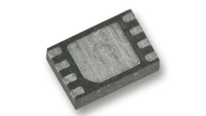
ToggleFLASH memories are one of the integrated or embedded semiconductor devices, aimed at helping the consumer electronics with excellent data storage. MT25QL128ABA1EW7-0SIT is one of such FLASH memories but it has an additional feature – it supports the SPI interface.
In our article today, we dive deeper into what this memory type does. We also cover some of the properties, as well as the overall advantage of the FLASH memory.
What is FLASH Memory?
It is a type of non-volatile storage system that is easy to reconfigure or modify for other purposes. Wikipedia has it that a FLASH memory, aside from making data or wireless information storage easy for consumer electronics, can also be electrically reprogrammed or erased.
Arguments have been made on the relevance of the erasing capability, seeing that the major goal of using a memory is to store information. It is on this premise that a solution was created via the demarcation of the FLASH memory types.
Today, we generally have two (2) types of variants, which are the NAND Flash and the NOR Flash. MT25QL128ABA1EW7-0SIT belongs to the latter because it is a serial NOR Flash memory.
How Does the MT25QL128ABA1EW7-0SIT NOR Flash Memory Operate?
The major difference between the NOR Flash Memory and the NAND Flash Memory is that the former makes an individual assessment of the memory cells. This assessment paves the way for the data not to be based on sequences. On the other hand, the NAND Flash Memory type doesn’t allow for a direct access to the individual memory cells.
The Security Registers
Besides enabling real-time data reading and writing (and the erasing too); MT25QL128ABA1EW7-0SIT allows for the respective registers to function effectively. An example is the set of registers categorized as the security registers. These are in place to keep the data safe.
Below are some of the components and how they combine to make the data safety worth it:

1. Volatile Lock Bits
The primary goal of the security registers is to enable both password and sector protection as measures for protecting the data. The registers also combine the bit settings, and a combination of the volatile and the non-volatile registers to enable this password and sector protection on multiple levels.
Now, the volatile lock bits are one of such bit settings used for this purpose. It works by making a temporal locking of the individual memory sector – after the latter must have been provided with a volatile protection.
In light of this, the locked or protected individual memory sector would only have the protection or safety feature removed after the device has been powered down/off or reset.
2. Sector Protection Register
This is the primary security register that enables MT25QL128ABA1EW7-0SIT’s memory protection. The sector protection sector is used to “protect the sector” via the use of two active bits, and a 16-bit non-volatile register to activate both the password and sector protection features.
3. Non-Volatile Lock Bits
This is also one of the bit settings used to secure MT25QL128ABA1EW7-0SIT’s individual memory cells. It works by using the non-volatile bit to correspond to and provide a non-volatile protection for the individual memory sector.
Worthy of mentioning is that the individual memory sector remains locked, except the corresponding bit is “cleared” and reset to the value, “1.”
4. Global Freeze Bit
While the bit settings and the register talked about above are used to make individual programming for the individual memory sector; the global freeze bit is not used for an individual purpose. Instead, this bit settings are activated to protect all the subsisting settings in all of the non-volatile lock bits.
Multi-Erase Capabilities
As an erase-centric NOR Flash Memory, MT25QL128ABA1EW7-0SIT supports multiple erasing options. These options include but are not limited to:
- Subsector erase of 4KB, with a 32KB granularity.
- Sector erase 64KB, with uniform granularity.
- Bulk erase
MT25QL128ABA1EW7-0SIT Supports Several Protocols
MT25QL128ABA1EW7-0SIT’s support for multiple protocols is based on the fact that these protocols are to work in both the DTR and the STR.

The list of supported protocols includes:
- Quad I/O protocol
- Extended I/O protocol
- Dual I/O protocol
Why NOR Flash Memory?
Since MT25QL128ABA1EW7-0SIT uses the NOR variant of the FLASH memory, is there any reason for that? These are some of the memory’s benefits:
5. The Non-Volatility is a Huge Bonus
Reading, writing, erasing and transfer of data is important in a consumer electronic and that is what the memory provides.
However, NOR Flash being a non-volatile memory type makes it better because it means that the data or content can be permanently stored, irrespective of whether the device is connected to a power source or not.
6. The Emphasis is on the Bytes
Without generalizing the data, it is now easier to find out whether the data is accurate or not. Thus, the focus of MT25QL128ABA1EW7-0SIT’s NOR Flash Memory is typically on the individual memory bytes and not the entire memory cells.
7. Fast Data Access
The data or wireless information stored in MT25QL128ABA1EW7-0SIT can be accessed in real-time, thanks to the speedy design.
Because the NOR Flash Memory does not arrange the data cells in a parallel manner, it means that the data cells can now be accessed easily.
8. Reprogramming is of the Essence
Aside from getting erased, the data cells in MT25QL128ABA1EW7-0SIT can also be reprogrammed or made into other relevant models.
9. The NOR Flash is a Dense Memory
More and more consumer electronics are using the smallest of memory sizes and that is in line with the growing demands for circuits that do not take up much space.
It is therefore, pertinent to ensure that the circuit or electronics’ components are also small in size.
The NOR Flash Memory minimizes the data cells’ path because of the space or size miniaturization, as it is “dense.” Being dense, as used here, means that the memory doesn’t take up much space.
Despite the smaller size, the NOR Flash “dense” memory can also accommodate more data.
Final Thoughts
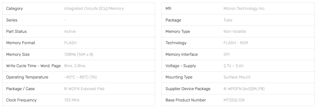
MT25QL128ABA1EW7-0SIT has a fast data write time, estimated at 8ms, 2.8ms write cycle time and word per page.
If you are using this memory, you can be sure that it wouldn’t take up much space, it would store plenty of data and still support a 133 MHz clock frequency.


