PCB assembly flexible is a technology that has revolutionized the electronics industry. The development of flexible printed circuit boards has allowed for the creation of smaller and more complex electronic devices. The use of flexible PCBs has become increasingly popular due to their ability to be bent or folded, making them ideal for use in wearable technology, medical devices, and other applications where flexibility is essential.
Flexible PCBs are made from a thin, flexible material that can be bent, folded, or twisted without breaking. They are composed of multiple layers of copper and insulating material, which are laminated together to form a flexible circuit board. The flexibility of these boards allows for the creation of compact and complex electronic devices that were previously impossible to create with traditional rigid PCBs.

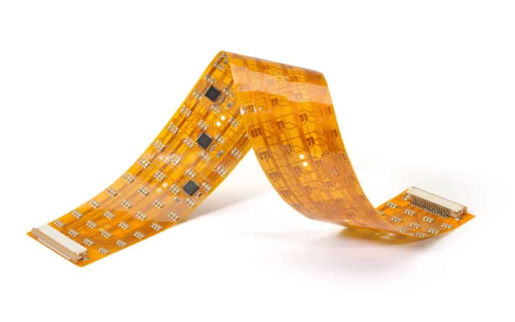
PCB Assembly Flexible: An Overview
PCB Assembly Flexible is a type of printed circuit board that can be bent, twisted, or folded to fit into a variety of shapes and sizes. It is a popular choice for applications that require flexibility, such as wearable technology, medical devices, and automotive electronics.
Flexible PCBs are made from a thin, flexible substrate material, typically a polymer or a combination of polymers. These substrates can be made to bend and flex without damaging the circuitry, making them ideal for applications that require frequent movement or vibration.
PCB Assembly Flexible can be designed to have multiple layers, just like traditional rigid PCBs. This allows for complex circuits and components to be integrated into a single, flexible board.
One of the main advantages of PCB Assembly Flexible is its ability to reduce the overall size and weight of electronic devices. Because the board can be shaped to fit the available space, it can be used in applications where traditional rigid PCBs would not fit.
In addition to their flexibility, PCB Assembly Flexible also offer other benefits such as improved signal integrity, reduced electromagnetic interference (EMI), and increased reliability due to fewer interconnects and solder joints.
Overall, PCB Assembly Flexible is a versatile and reliable option for a wide range of electronic applications, particularly those that require flexibility and space-saving design.
Advantages of PCB Assembly Flexible
Improved Flexibility
One of the main advantages of PCB assembly flexible is the improved flexibility it offers. Unlike rigid PCBs, flexible PCBs can bend and twist, allowing them to fit into tight spaces and follow the contours of the product they are being used in. This makes them ideal for use in products that require a high degree of flexibility, such as wearable technology, medical devices, and automotive components.
Higher Density
Another advantage of PCB assembly flexible is the ability to achieve higher density. Flexible PCBs can be designed with smaller components and tighter spacing, allowing for more circuits to be packed into a smaller area. This makes them ideal for use in products that require a high level of functionality in a small space, such as smartphones, tablets, and other portable devices.
Cost-effective
Flexible PCBs can also be more cost-effective than rigid PCBs. Because they can be designed to fit the specific shape and size of the product they are being used in, there is less waste material and fewer assembly steps required. This can result in lower production costs and faster turnaround times, making them a popular choice for manufacturers looking to reduce costs and increase efficiency.
In conclusion, PCB assembly flexible offers a number of advantages over traditional rigid PCBs, including improved flexibility, higher density, and cost-effectiveness. These benefits make them an ideal choice for a wide range of products, from wearable technology to medical devices and more.
Types of PCB Assembly Flexible

Single-sided Flex PCBs
Single-sided flex PCBs are the simplest type of flexible PCBs. They consist of a single layer of conductive material on a flexible substrate. These PCBs are typically used in applications where space is limited, and the board needs to be able to bend or flex. Single-sided flex PCBs are often used in consumer electronics, such as smartphones, tablets, and wearables.
Double-sided Flex PCBs
Double-sided flex PCBs have two layers of conductive material on a flexible substrate. These PCBs are used in applications where more complex circuitry is required, but space is still limited. Double-sided flex PCBs are often used in medical devices, aerospace, and automotive applications.
Multilayer Flex PCBs
Multilayer flex PCBs have three or more layers of conductive material on a flexible substrate. These PCBs are used in applications where complex circuitry is required, and space is limited. Multilayer flex PCBs are often used in military, aerospace, and medical applications.
In conclusion, there are three main types of PCB assembly flexible: single-sided flex PCBs, double-sided flex PCBs, and multilayer flex PCBs. Each type of PCB has its own unique advantages and disadvantages, and the choice of which type to use depends on the specific application.
Design Considerations for PCB Assembly Flexible
Flexibility and Bending Radius
Flexibility and bending radius are crucial factors to consider when designing a flexible PCB assembly. The bending radius determines the minimum bend radius that a PCB can withstand without damaging the circuit. PCBs with smaller bending radii are more flexible and can be bent more easily. However, they are also more susceptible to damage and breakage.
To ensure the reliability and durability of a flexible PCB assembly, it is important to choose a bending radius that is appropriate for the application. The bending radius should be large enough to prevent damage to the circuit, but small enough to allow for the desired level of flexibility.
Stack-up and Layer Count
The stack-up and layer count of a flexible PCB assembly can have a significant impact on its performance and reliability. The stack-up refers to the arrangement of the layers in the PCB, while the layer count refers to the total number of layers.
When designing a flexible PCB assembly, it is important to choose a stack-up and layer count that is appropriate for the application. The stack-up should be optimized to minimize signal loss and interference, while the layer count should be chosen to provide the necessary functionality and performance.
Connector Placement
Connector placement is another important factor to consider when designing a flexible PCB assembly. The location and orientation of connectors can have a significant impact on the performance and reliability of the circuit.
To ensure optimal performance and reliability, connectors should be placed in locations that are easily accessible and can withstand the stresses of bending and flexing. Additionally, the orientation of connectors should be chosen to minimize signal loss and interference.
In conclusion, when designing a flexible PCB assembly, it is important to consider factors such as flexibility and bending radius, stack-up and layer count, and connector placement. By carefully considering these factors, it is possible to create a reliable and high-performance flexible PCB assembly that meets the needs of the application.
Manufacturing Process for PCB Assembly Flexible
Material Selection
The first step in the manufacturing process for PCB assembly flexible is material selection. The choice of materials is important to ensure the final product meets the required specifications. The materials used for flexible PCBs are typically polyimide or polyester films, which are chosen for their flexibility, durability, and thermal stability. Copper is used for the conductive traces, and adhesives are used to bond the layers together.
Etching and Imaging
The next step is etching and imaging. This involves creating the circuit pattern on the copper layer using a photolithography process. The copper layer is coated with a photoresist material, which is then exposed to UV light through a mask. The areas that are not exposed to light are then washed away, leaving behind the circuit pattern. The exposed copper is then etched away, leaving only the circuit traces.
Drilling and Plating
After etching and imaging, the next step is drilling and plating. Holes are drilled in the PCB to allow for the insertion of components. The holes are then plated with copper to ensure a good electrical connection between the layers. This is done by placing the PCB in an electroplating bath, which deposits a thin layer of copper on the walls of the holes.
Assembly and Testing
The final step is assembly and testing. Components are placed on the PCB using automated pick-and-place machines. The PCB is then heated to bond the components to the board. The final product is then tested to ensure it meets the required specifications. This includes testing for continuity, insulation resistance, and functionality.
In conclusion, the manufacturing process for PCB assembly flexible involves material selection, etching and imaging, drilling and plating, and assembly and testing. Each step is important to ensure the final product meets the required specifications.
