Flex PCB design needs a little different approach in contrast to the rigid PCBs. Though the flex PCBs can offer huge savings in the manufacturing space, lower weight, as well as reduced space consumption, there is a need to make their banner design optimized for the use cases as well as their materials.
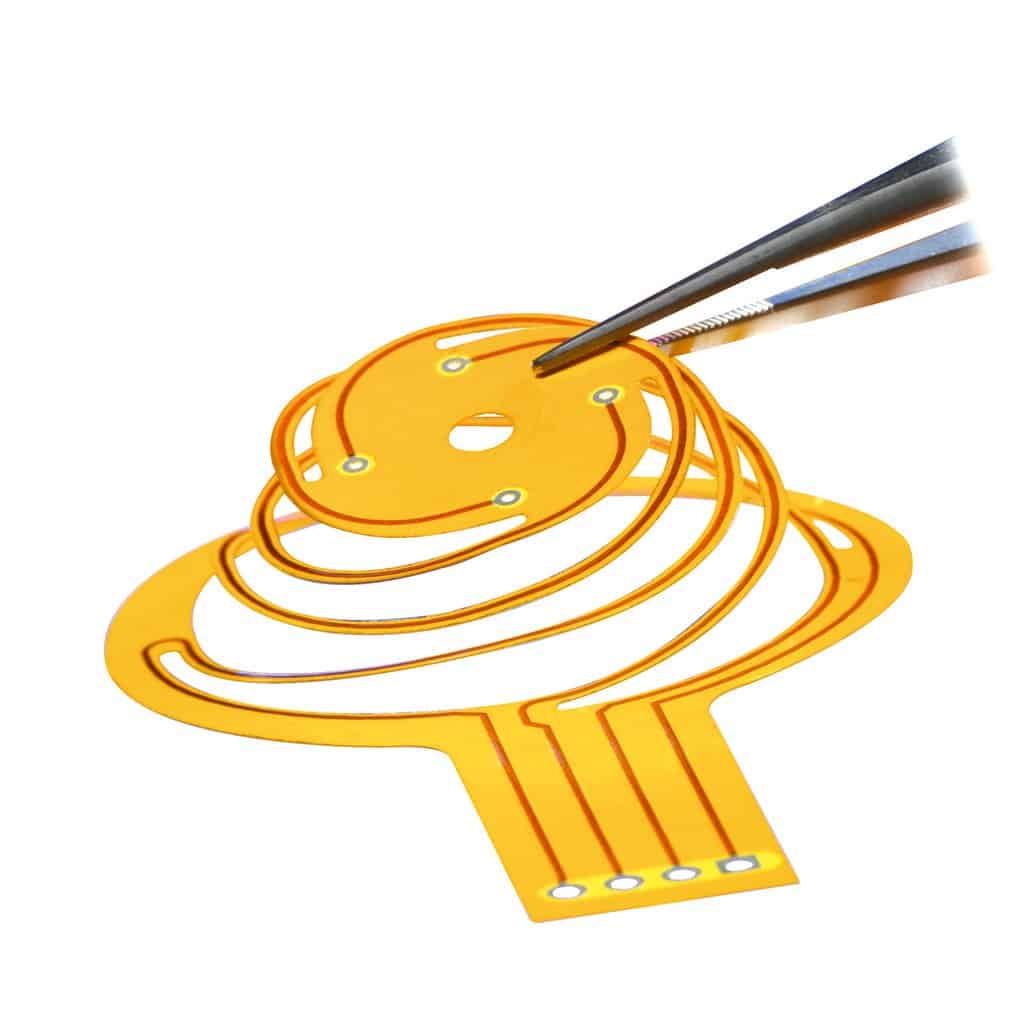
A flex PCB with a banner design will be easily installed, durable, lightweight, and appropriate for very demanding applications like satellites and wearable devices. The flex’s physical advantages are that it provides an improved resistance to possible movement and vibrations. Also, preparing it for the harsh environments is easier.
There are many ways to make sure you have a high quality flex PCB design. Now, let us take a look at those things you should know during your Flex PCB board design.
Important Things to Know for your First Flex PCB Board Design
Understanding the flexibility/bendability of the Flex PCB
There are two important things you should know regarding flexibility. First, how many times will this PCB be flexing? Second, what extent will this PCB flex? The times at which it will be able to bend or the application, will determine if the board should be a dynamic board or a static board. The static board is usually viewed as the bend-to-install. Also, it usually flex below 100 times throughout its lifetime.
Furthermore, the design of the dynamic board will have to withstand so many bends (say tens of thousands). In addition, these PCBs are great for extremely harsh conditions like military and spacecraft applications.
The bend radius is the least quantity of bendiness for that flex area. Also, it has to be identified properly very early during the banner design. With this, the banner design will permit the required number of leads without bringing any damage to the copper.
During the laying out of these bend areas, prevent the 90-degree bends, which causes high strain. The plated through holes must be avoided in your bend area, and the conductors have to be staggered in the multilayered circuits. This is to ensure greater effectiveness.
Also, conductors that are less than 10 mils have to be placed in its neutral bend axis where no compression or tension is present all through the flexing process. One significant feature of flexibility of flex PCBs is flexibility. This enables PCB designers to make use of them in very tiny packages.
Heat Forming Flex PCBs
The heat forming feature usually needs the steel jig. This is because it makes the board lie in a specific way. You then insert this steel jig into the oven. One important benefit of the heat forming feature is that it offers a tighter bend radius. Moreover, the heat forming is useful mainly for easy installation. The tighter and stronger bend radius usually seems to be an extra capability that it offers.
Slots and Cutouts Present in Bend Region
When there are no traces present in our bend region, then you can minimize the radius. This is achievable by inserting slots or cutouts. Making use of cutouts help in reducing the quantity of material that is necessary for bending. Also, the other option is to get rid of the flex sections that have no circuitry. Though you have to get rid of this lengthwise and this will need routing afterwards.
Knowing the Flex PCB Materials
The major material that is useful for both the coverlay layers and the flex layers is Polyimide. The flex materials help in providing more effective material properties in contrast to the rigid PCBs. In addition, the flex materials thickness is uniform and it features a better Dk value that falls within the range of 3.2 and 3.4.
In the absence of the oven, glass reinforcement helps in getting rid of any variations present in the dielectric constant (Dk). Also, the polyimide is extremely thick when it comes to the thickness as a result of the cast manufacturing process.
The layer thickness falls within the range of 0.5 – 4 mils. The cladding of the polyimide flex core is achieved with rolled annealed copper or electro-deposited copper. It is an extremely thin copper and works great for both static and dynamic applications. The 0.7 mils (0.5 oz) copper is usually used for the flex PCBs. Furthermore, the very common copper weights for the flex PCB are 1oz and 0.5oz. Also, 2oz is the higher copper weight. With this, you will get the most appropriate combinations of the thinnest construction.
Two main flex material types are available. First is the adhesive-based, whereby the polyimide bonds to the copper with the acrylic adhesive. The second is the adhesive-less, whereby the copper is directly cast on the polyimide.
Watch the Flex Trace Routing Closely
The circuitry layout helps in breaking or making the PCB (printed circuit board). It is better to make use of a large radius here rather than the sharp angles which reduces the lifespan of the board. However, you should avoid any I-beaming. This will help in minimizing the stress, which could end up thinning out the copper circuits.
The curved traces lead to lower stress in contrast to the angled ones. Also, the traces must be made to stay perpendicular with respect to the general or overall bend. Also, when you place it on the flex PCB having at least two layers that are staggered both at the bottom and top.
Guidelines for the Rigid Flex PCB
Early during the design process of the rigid flex PCB, it is very important that you give enough consideration to the way the choices are made all through the board design. This leads to reduced costs coupled with maintaining reliability. In this article, we will be laying out the general principles and PCB design tips that ought to guide the designer when working on the rigid flex PCBs.
What are Rigid Flex Boards?
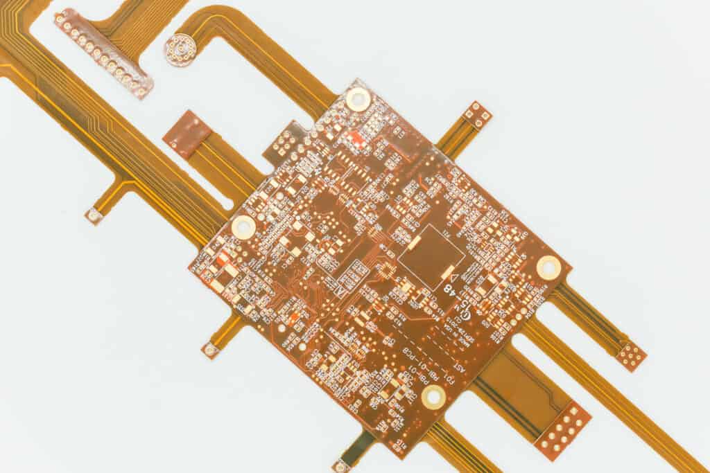
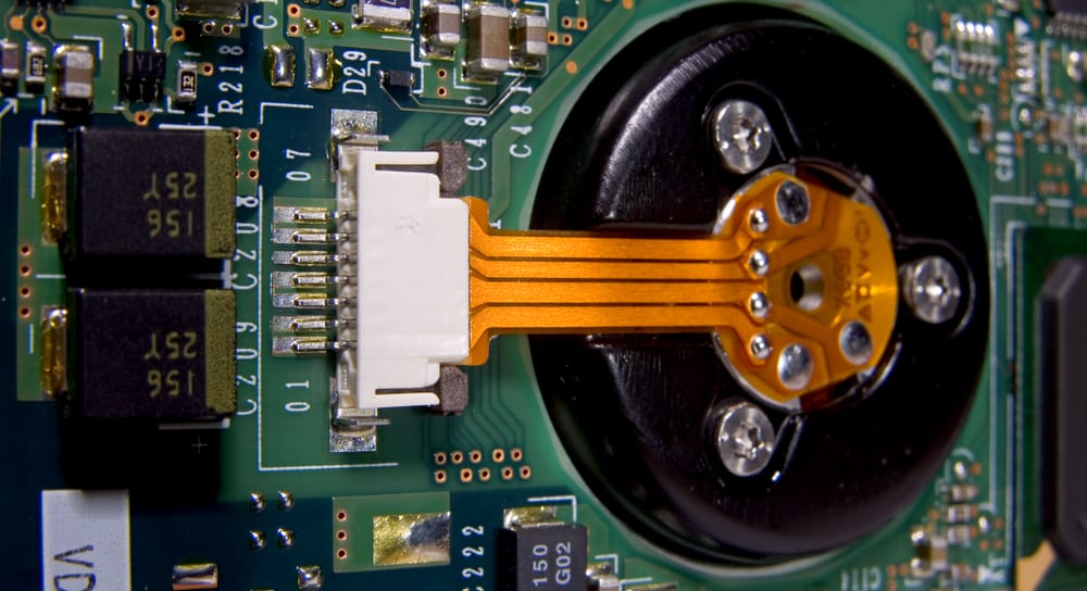
Rigid flex boards are a hybrid of the flexible and hardboard circuits. The process of manufacturing here is similar to that of the traditional hardboard circuit. However, some layers are the flexible circuitry which runs all through the hardboard. The board fabricator then adds the plated through holes. This helps in connecting the rigid circuit layers to the flexible circuit regions.
In addition, these configurations help in the creation of the rigid flex PCB, which you can assemble just like the hardboards. It also folds to help in fitting in a product having space constraints.
Rigid Flex PCB Design Guidelines
Speaking broadly, the rigid flex design usually looks closely like the hardboard design. Its flexible layers fully extend to the board’s rigid layers. Just like the hardboard layouts, the package for rigid flex fabrication includes the gerber layers, solder mask layers, drill files, coverlayer, rout/perimeter files, and more.
Moreover, some major differences exist in the fabrication process of the hardboard applications and the rigid flex PCB.
Generally, the rigid flex PCB print features more dimensions, and has to define the requirements carefully. This is because they are useful in different 3D applications. Also, it has to define the transition areas from rigid to flex as they are not usually obvious when viewing only the gerber layers.
The material layup present in the rigid flex boards is usually critical, and there’s a need to work with your fabricator regarding this.
Also, the rigid flex design boards need extra layers in your gerber files. The layers X and 1 will include the solder mask layer. However, there will be a need for the artwork layers. This helps in defining the bondply and coverlayer sections of the board. Also, it indicates how much each of them enters the hardboards.
Considerations for the Material Layup
The material layup of the rigid flex influences the cost, assembly process, manufacturability, and the end PCB performance. Therefore there is a need to take some time to determine the best material set. For example, resistance, controlled impedance, current-carrying requirements are very significant considerations, which affects the choice of material and copper weights.
The PCB designer has to work with the board fabricator to help in discussing these variables. This ensures that the eventual banner design works with all the requirements for signal integrity. Immediately the designer os through with performing the initial calculations, your fabricator will verify them and then make an accurate modeling of your circuit board’s impedance characteristics.
The rigid flex boards have rigid sections that are usually above 20 layers max. At times, they could have more, but this is usually very rare. These sections of hard board don’t always feature a similar layer count.
Furthermore, once the material layup is somehow similar for each board and they have the same thickness overall, then you shouldn’t experience any manufacturing issues. Also, at times, the design may include hardboards different in thickness. However, manufacturing these configurations are more difficult, and so other options have to be considered.
Conclusion
The design of Flex PCB needs a little different approach in contrast to the rigid PCB. Although these flex PCBs can offer huge savings in the manufacturing space, there is a need to make their banner design optimized for the use cases. If you want us at Rayming PCB, you can contact us or reach us on our various social media channels.
