PCB layout power amplifier is an essential aspect of electronic circuit design. The PCB layout is a critical part of the design process that can have a significant impact on the performance of the amplifier. It is crucial to ensure that the layout is optimized for the specific requirements of the amplifier to achieve the desired performance.
The PCB layout of a power amplifier is designed to provide the necessary electrical connections between the components of the circuit. It is essential to ensure that the layout is optimized for the specific requirements of the amplifier to achieve the desired performance. The layout must be designed to minimize noise, crosstalk, and other undesirable effects that can degrade the performance of the amplifier. It is also important to ensure that the layout is compatible with the manufacturing process to ensure that the final product is reliable and cost-effective.
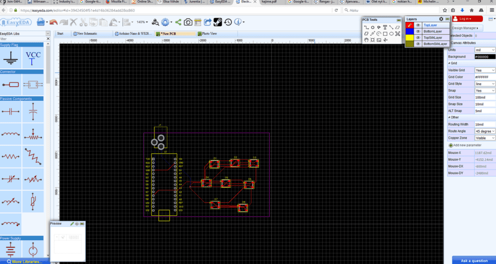
PCB Layout for Power Amplifier
Power Amplifier Basics
A power amplifier is an electronic device that amplifies the power of a signal. It is used to drive a load, such as a speaker or motor. The power amplifier typically consists of several stages, including the input stage, the driver stage, and the output stage. The input stage is responsible for amplifying the signal from the source, such as a microphone or guitar. The driver stage amplifies the signal further and provides impedance matching. The output stage is responsible for delivering the power to the load.
PCB Design Considerations
When designing a PCB layout for a power amplifier, there are several factors to consider. These include the size of the PCB, the placement of components, the routing of traces, and the use of ground planes. The size of the PCB should be large enough to accommodate all of the components and traces without overcrowding. The placement of components should be carefully planned to minimize noise and interference. The routing of traces should be kept as short as possible to minimize losses and crosstalk. The use of ground planes can help to reduce noise and interference.
Power Amplifier PCB Layout Techniques
There are several techniques that can be used to optimize the PCB layout for a power amplifier. These include the use of star grounding, the placement of decoupling capacitors, and the use of thermal vias. Star grounding involves connecting all of the ground points to a single point to minimize ground loops. Decoupling capacitors are used to filter out noise and interference. They should be placed as close as possible to the power supply pins of the components. Thermal vias are used to dissipate heat from the components to the ground plane.
In summary, designing a PCB layout for a power amplifier requires careful consideration of several factors. The size of the PCB, the placement of components, the routing of traces, and the use of ground planes are all important considerations. Techniques such as star grounding, decoupling capacitors, and thermal vias can be used to optimize the layout and improve performance.
Power Amplifier PCB Layout Techniques

When designing a power amplifier PCB layout, there are several key techniques to consider to ensure optimal performance and reliability. These include grounding techniques, component placement, power supply decoupling, and thermal management.
Grounding Techniques
Grounding is critical in power amplifier design, as it helps to minimize noise and interference. One effective technique is to use a star grounding scheme, where all ground connections are routed to a single point. This can help to reduce ground loops and improve overall signal integrity.
Component Placement
Careful component placement is essential for minimizing noise and maximizing performance. Key components, such as the power supply, should be placed as close as possible to the power amplifier circuitry to minimize voltage drops and reduce noise. Additionally, it is important to keep high-frequency components, such as capacitors and inductors, separated from one another to prevent unwanted coupling.
Power Supply Decoupling
Power supply decoupling is crucial for reducing noise and ensuring stable operation. Decoupling capacitors should be placed as close as possible to the power amplifier circuitry to minimize inductance and resistance. It is also important to use multiple capacitors of varying values to cover a wide range of frequencies.
Thermal Management
Heat is a major concern in power amplifier design, as excessive temperatures can lead to component failure and reduced lifespan. Proper thermal management techniques, such as using heat sinks and thermal vias, can help to dissipate heat and improve overall reliability.
By implementing these key techniques, designers can create power amplifier PCB layouts that deliver optimal performance and reliability.
Component Placement
Placement Considerations
When designing a PCB layout for a power amplifier, the placement of components is crucial for optimal performance. The placement of components can affect the overall performance, efficiency, and stability of the amplifier. Here are some considerations to keep in mind when placing components:
- Keep the power supply traces as short as possible to minimize voltage drop and noise.
- Place the input and output connectors far away from each other to reduce the possibility of oscillation.
- Place the power amplifier as close as possible to the output connector to reduce the output trace length.
- Avoid placing components near the heatsink to prevent interference with heat dissipation.
Component Layout Guidelines
When placing components on the PCB, there are some general guidelines that can help ensure a successful layout.
- Group components according to their function to minimize the length of signal traces and reduce the possibility of interference.
- Place the power supply components near the power amplifier to minimize voltage drop and noise.
- Place the input and output components as close as possible to the input and output connectors to minimize signal loss.
- Use a ground plane to reduce noise and improve signal integrity.
- Place decoupling capacitors as close as possible to the power pins of the amplifier to minimize noise.
By following these guidelines and considerations, you can create an optimal layout for your power amplifier PCB. Remember to keep the layout as compact as possible while still maintaining sufficient space between components to prevent interference.
Grounding Techniques

Ground Plane
One of the most important aspects of a PCB layout for a power amplifier is proper grounding. A ground plane is a large area of copper on the PCB that is connected to the ground of the circuit. It is used to provide a low impedance path for ground currents and to reduce the amount of noise in the circuit. The ground plane should cover as much of the PCB as possible, leaving only small gaps for signal traces to pass through.
Star Grounding
In addition to a ground plane, a power amplifier circuit should also use star grounding. This technique involves connecting all of the ground points in the circuit to a single point, rather than daisy-chaining them together. This helps to reduce ground loops and minimize the amount of noise in the circuit.
When implementing star grounding, it is important to ensure that the ground point is located as close as possible to the power supply ground. This will help to minimize the impedance of the ground path and reduce the amount of noise in the circuit.
Another important consideration when using star grounding is to ensure that the ground traces are as short as possible. This will help to minimize the inductance of the ground path and reduce the amount of noise in the circuit.
Overall, proper grounding techniques are essential for a successful PCB layout for a power amplifier. By using a ground plane and star grounding, designers can minimize noise and ensure that the amplifier operates at its full potential.
Power Supply Decoupling
Decoupling Capacitor Selection
The selection of decoupling capacitors is critical in ensuring that the power amplifier circuit functions optimally. Decoupling capacitors are used to reduce the noise and ripple in the power supply, which can cause unwanted distortion in the output signal.
The capacitance value of the decoupling capacitor is important and should be selected based on the frequency range of the amplifier circuit. For high-frequency circuits, a smaller capacitance value is required, while for low-frequency circuits, a larger capacitance value is necessary.
In addition, the type of capacitor used is also important. Ceramic capacitors are commonly used for decoupling due to their low ESR and ESL. However, tantalum and electrolytic capacitors can also be used for decoupling.
Decoupling Capacitor Placement
The placement of decoupling capacitors is also crucial in ensuring that the power amplifier circuit functions optimally. Decoupling capacitors should be placed as close as possible to the power pins of the amplifier IC.
In addition, multiple decoupling capacitors can be used to further reduce noise and ripple in the power supply. A combination of ceramic, tantalum, and electrolytic capacitors can be used for decoupling, with the ceramic capacitors placed closest to the amplifier IC.
It is also important to ensure that the ground connections of the decoupling capacitors are as short as possible to minimize the inductance in the circuit.
Overall, proper decoupling capacitor selection and placement is critical in ensuring that the power amplifier circuit functions optimally, with minimal noise and distortion in the output signal.
Thermal Management
Thermal Considerations
Thermal management is an important aspect of designing a PCB layout power amplifier. The power amplifier generates heat, and it is important to dissipate this heat efficiently to avoid damaging the components and causing the amplifier to malfunction.
The thermal considerations for a PCB layout power amplifier include the maximum operating temperature of the components, the thermal resistance of the components, and the maximum allowable temperature rise. It is important to select components that can handle the maximum operating temperature and to minimize the thermal resistance by using appropriate copper traces and vias.
Heat Sink Selection
A heat sink is a passive cooling device that helps dissipate heat from the power amplifier. The selection of a heat sink depends on the power dissipation of the amplifier, the ambient temperature, and the available space on the PCB.
There are different types of heat sinks available, including extruded, stamped, and folded fin heat sinks. The choice of heat sink depends on the specific requirements of the amplifier. Extruded heat sinks are suitable for high-power amplifiers, while stamped and folded fin heat sinks are suitable for low to medium power amplifiers.
Heat Sink Attachment
The heat sink must be attached to the power amplifier to ensure efficient heat dissipation. The attachment method depends on the type of heat sink and the available space on the PCB.
The most common methods of heat sink attachment include using thermal adhesive, screws, or clips. Thermal adhesive is suitable for small heat sinks, while screws and clips are suitable for larger heat sinks. It is important to ensure that the heat sink is securely attached to the power amplifier to avoid any movement or vibration that could damage the components.
In conclusion, thermal management is an important aspect of designing a PCB layout power amplifier. The thermal considerations, heat sink selection, and heat sink attachment are crucial to ensure efficient heat dissipation and avoid any damage to the components.
