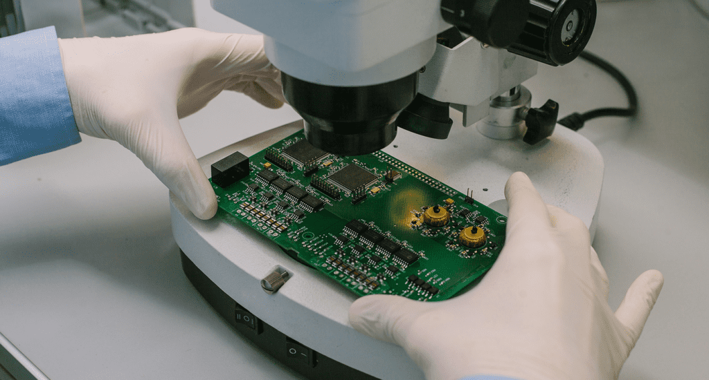
Over time, printed circuit boards have become a crucial element in the Electrical and Engineering Industry. Their main selling points are that they are slim, effective, durable, and function well even in harsh environments. Moreover, these components reduce the number of wires you utilize when creating a circuit, as they contain copper traces that efficiently transfer electrical signals. In doing so, these components help manufacturers develop pretty slim gadgets, for example, a smartphone. However, though PCBs are pretty effective in terms of functionality, creating them can be a great hassle.
The PCB designing and Assembly process are procedural, and manufacturers must follow a specific trend to generate effective PCBs. Moreover, PCB designs, unlike other plans, for example, architectural blueprints, tend to be pretty tricky to develop, and messing them up could ruin the final product. Furthermore, how your Printed Circuit Board will perform will mostly depend upon the configurations you utilize on the board. Therefore, when developing a PCB, you must consider all these points if you wish to create a PCB that will not fail you. But how can you ensure that you will continually develop a functional PCB? And how can you perfect the Printed Circuit Board design and assembly process?
Designing your Printed Circuit Board
A Poor PCB design can lead to you developing a circuit board that has reliability and functional problems. Therefore, to avoid causing needless hassles and going over budget to fix a design stage error, you should always ensure that your PCB design is perfect. And the first step towards ensuring that you develop a perfect PCB design is creating a PCB layout before you work on the actual design. The layout will guide you efficiently during your PCB design process and ensure that you develop the best design without messing things up.
Moreover, during the layout development stage, you can also cover definition, ideation, and validation. Doing so will help you discover whether or not you can further improve your PCB design while still staying within the budget. Moreover, these three steps will also help you improve the compatibility between all the components you will fix on your PCB. And the more compatible the components in your board are, the more functional the board will be. Therefore the final product will be great.
Pre-emptive Knowledge Sharing
If you wish to develop a perfect PCB design using the shortest possible time, you should not skip the pre-emptive knowledge-sharing stage. In this stage, members of your PCB designing team will bring in good ideas to help you develop a good PCB design. Moreover, depending on their ideas, you can get to know the team members that are all in and those that are only in it for the money.
You should also develop a firm-up timeline and a budget to help you manage the designing phase. Doing so will help guide you into creating a cost-friendly PCB.
Printed Circuit Board Design basics, Things that you should Greatly Consider
Before we move on to the various Printed Circuit Board designing practices, let us first cover what you have to keep in mind when developing a PCB design to help you cut costs and create a functional PCB.
Components
When developing a PCB design, ensure you utilize materials that manufacturers can find with ease. However, if you decide to work with niche parts, then you should be ready to pay extra to get the job done. Moreover, manufacturers tend to take more time to find niche parts. Hence you can expect production delays which will also boost the amount of money you spend.
Placement
Placement is another crucial factor to consider when working with a Printed Circuit Board. That is because if you mess up component placement details at the designing stage, manufacturers will have a hard time during soldering and component rotation. These issues will ultimately drive your board’s production cost up immensely.
Printed Circuit Board Layout
When developing a PCB layout, avoid generating a complex one. That is because a complicated PCB layout will lead to a complex circuit board assembly process which will cost you more. Therefore, you should instead go with a simple Printed Circuit Board layout. However, it would help if you kept the functionality factor in mind even when developing a simple layout. For instance, you should ask yourself questions like, will your PCB design connect to interfaces? Doing so will help you avoid last-minute surprises that will cost you more money to fix.
How to Efficiently Develop a Functional PCB Design

Now that you have tips on how to cut some costs and still produce a functional PCB design, let us focus on how to create the actual layout and PCB prototype. To do so, you should follow the steps below:
Select a Good Printed Circuit Board Designing Software
Manually designing a PCB is, without a doubt, an old thing to do. However, these days Printed Circuit Board designers rely on PCB designing software programs to develop efficient, high-quality, pro-like designs. Moreover, these software programs contain multiple tools to help you generate your design without breaking a sweat.
However, not all PCB designing software programs are efficient in terms of helping you develop an optimized PCB design. For instance, a perfect PCB designing software should be able to let you draw both Printed Circuit Boards and schematics. If a PCB designing software does not offer you these options, you should opt to utilize another program.
Examples of the most common PCB designing software programs that you will find in the market today include:
– gEDA-project
– KiCad
– Cadsoft Eage
Moreover, you can also utilize CAD libraries to help you optimize the designing phase; they are pretty helpful.
Avoid concentrating many Components in a Small Area, and Consider the Board’s Fabrication
While developing a PCB design, think about the board’s soldering and general assembly process. Will the soldering process be too complex? And will the assembly procedure of your PCB be too complex, or will it be simple? Remember that complex designs are a hassle to bring to life, which is unsuitable for your budget.
Therefore, you should always ensure that you distribute the PCB components fairly on the board. Moreover, when developing the design, avoid including buried and blind vias. These types of vias tend to be tricky to curve out. Therefore they will automatically make your design complex.
Trace Width Calculation
Your board’s trace width will play a significant part in determining whether or not the board design is optimal. Therefore, instead of blindly selecting a trace width out of the blues, you should try to work with a trace width calculator.
A printed Circuit Board width calculator helps you determine how wide and thick your board’s trace should be. However, to ensure optimal performance, you should aim to hit a 50C or 410 temperature rise. But if your board is large, you can still work with a bigger trace.
Trace width calculators are free to use. Therefore you can utilize them without worrying about going over budget.
Through Holes or Surface Mount Tech?
When developing a PCB, you will realize that if you go with SMT or surface mount Tech, you will spend less time and money. However, if you decide to utilize through hole, you should be ready to pay more cash and spend more time producing your PCB.
But, if your PCB will function under environmental and mechanical stress, you might not have a choice but to work with THT. That is because THT tends to produce more persistent PCBs that can survive under intense stress. Therefore, choosing between THT and SMT depends on how you wish to use your PCB.
However, you can also utilize SMT and THT together to produce a hybrid PCB.
Circuit Board Patterns
The easiest error you can make while producing a PCB design is messing up the board’s circuit pattern. Remember that if you miscalculate your board’s pad-to-pad spacing and go off course by even 70 microns (or the size of a human hair), the PCB’s pins will not align during production. And with this misalignment in place, applying solder mask will be challenging to accomplish, if not impossible.
To avoid making such an error, you should utilize PCB design software that bears an electronics component library. Moreover, the library must include the following:
– Schematic symbols and,
– Printed Circuit Board landing patterns (for each of the board’s components)
You should be on the safe side by sticking to this crucial component when developing your PCB design.
However, if you decide to work on your PCB design manually, you should start by sketching the board landing pattern and schematic before you start to draw the actual design. But remember, when working on your design manually, the chances of messing up tend to be pretty high; hence you should be extra careful when sketching everything.
Ensure all the necessary Components Fit Perfectly on the Circuit Board
To make sure that all the essential components fit on your circuit board design, try to print your board design to a one is to one scale. Doing so will provide you with a view that is pretty realistic. From this view, you can judge the component placement distribution and make necessary adjustments.
Decoupling Capacitor Placement
When developing your PCB design, place the decoupling capacitors close to the ground and power pins. Doing so will automatically boost your board’s decoupling efficiency. On the hand, if you put the capacitors far from the ground and power pins, you will ultimately bring unwanted inductance into the PCB. Doing so will make the board inefficient and less optimal in terms of performance.
Optimize Switch Regulators
When developing a PCB design, you ultimately have to choose between two electronic components voltage regulators, namely:
– Switch regulators
– Linear regulators
Linear regulators tend to be pretty inexpensive to implement. Moreover, the process of laying them up is relatively simple when you compare it to the operation of laying up switch regulators. However, linear regulators have one downside, they tend to waste a lot of electrical power.
On the other hand, switch regulators are expensive and complex to implement, but they are great for applications requiring more power with minimal noise.
Avoid Buried and Blind Vias at all Costs
Buried vias connect two inner layers, while blind vias connect an internal layer to an external PCB layer. However, no matter the case, a PCB via must go through all the panels on a PCB to connect various traces from one board layer to another.
Though buried and blind vias are effective, they can make your PCB much thicker. Moreover, the manufacturer will charge you more money to produce the vias, putting a dent in your PCB production budget. Therefore, if your PCB can function appropriately without buried or blind vias, you should not use them.
PCB Designing Types (classification by material)
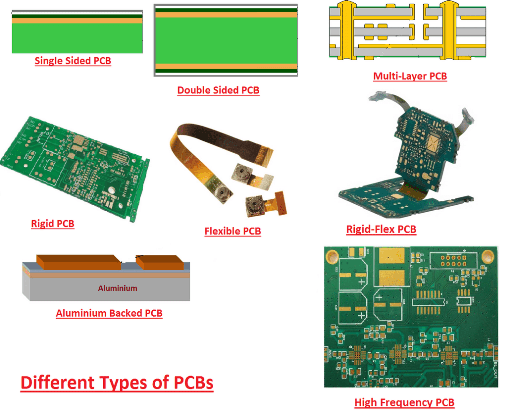
There are so many different Printed Circuit Board designs. However, the one that you choose solely depends upon how you wish to utilize your board.
The most common Printed Circuit Board designs in the market today include:
Flex Circuit Board Designs
Flex PCBs or flexible printed circuit boards are circuit boards that can bend are varying angles. Due to these flex factors, whichever material you utilize to design such a PCB should be bendable, and it should round up in different corners.
The materials of a flexible PCB are substrate materials (which are flexible) and copper. The manufacturer then combines these components using pressure, heat, and adhesive to make the flexible PCB.
Rigid-flex Circuit Board Design
As the name dictates, a rigid-flex printed circuit board is a circuit board that has both rigid and flexible characteristics. These types of PCBs are advantageous because they tend to have a hybrid characteristic, making them durable and effective. Moreover, they bear the advantages of rigid and flexible circuits.
Manufacturers primarily utilize rigid-flex printed circuit boards on cellphones since they tend to be pretty durable and effective. Moreover, manufacturers can easily manipulate the board design to make packaging less complex due to how the flexible part bends. Therefore, if you want to save space and still gain a durable PCB, you should choose this design.
Multilayer Circuit Board Design
A multilayer Printed Circuit Board is a board design bearing more than two layers. Moreover, the conductors of such a design bear three layers, each found at the center of the board’s material.
Multilayer Printed Circuit boards are crucial in the aerospace industry. Therefore, if your PCB is meant for aviation purposes, then you know the design to go with.
Moreover, multilayer printed circuit boards also function perfectly in:
– Repeaters
– Data storages
– Cell phone transmitters
– Computer
– File server
They are also helpful in various other applications, such as generating atomic accelerators, developing fire alarm controls, and building weather analysis machines.
Using a multilayer PCB design is pretty beneficial since these PCBs tend to be:
– Smaller in size
– Easy to incorporate into various gadgets
– Have increased flexibility
– Reduced interconnections
High-Speed Printed Circuit Board Designs
High-speed printed circuit boards have one thing in common, they all have an equipment signal interrupting characteristic. To make this characteristic possible, manufacturers manipulate the following physical elements:
– Interconnection
– Packaging
However, this type of design tends to be pretty complex, so if you decide to take it up, you should be ready to put in extra hours.
High power Circuit Board Design
When working on a PCB design, you should always adhere to one simple rule, the power path rule. Messing up your PCB’s power path could ultimately render your PCB useless.
Moreover, the amount of power and the location of your board’s circuit are two more factors you should consider when working on a PCB design. With these factors in check, you can easily produce a circuit design for a high-power PCB.
However, to optimize this design, you should also keep the following factors in check:
– The board’s ambient temperature
– Airflow in the circuit board
– IC density in the PCB
Moreover, the materials that you utilize to generate this type of PCB should be able to handle high temperatures with ease.
HDI Board Designs
HDI PCBs are becoming pretty popular in the circuit board industry. However, these types of PCBs bear buried/ blind vias and microvias, which have a small thickness of around 0.006 micrometers.
Moreover, these PCBs tend to bear a circuitry density that is pretty high when you compare them to standard PCBs. Actually, this circuitry density characteristic is the main selling point of these PCBs.
HDI circuit boards exist in six varying types, which are:
– PCBs bearing both buried and through vias
– PCBs bearing vias that pass through various surfaces
– Multilayer interconnects having high-density circuitries
– HDI printed circuit boards coreless construction, which uses layer pairs
– HDI PCBs with alternate construction – they utilize layer pairs
– Passive substrates
LED Circuit Board Designs
LED printed Circuit Boards are light-emitting diode (LED) PCBs. The primary function of these PCBs is to connect LEDs to a particular chip that delivers light. Whenever light passes through the PCB, the LEDs ultimately light up. The manufacturer can manipulate these circuit boards to perform different functions, for example, develop street lights and airport runway lights.
RF-printed Circuit Boards Designs
RF PCBs, or Radio Frequency Printed Circuit Boards, are pretty complex circuit boards manufacturers primarily utilize in smartphones, robots, and sensors. These PCBs are complicated to manufacture as they utilize the latest technology. Therefore, if you decide to utilize this design, you should be ready to use more money.
However, if your PCB has to function using a frequency that is 100MHz and above, then your circuit board will fall under this category.
Gadgets that work with RF Printed Circuit boards tend to be pretty complex, and they can work perfectly with both analog and digital signals.
High voltage Printed Circuit Boards
High-voltage Printed circuit boards are PCBs that can handle incredibly high voltages. However, if you opt to develop this PCB design, you need sufficient design space and proper clearance.
When developing such a design, you should have a few things in mind. These things include
– Basic insulation
– Reinforced insulation
– Supplementary insulation
– Functional insulation
– Double insulation
– Basic insulation
– Altitude
– Clearance
– Creepage clearance
Now that we have the designing tips out of the way, it’s time to look at some tips to help you have a smooth time during PCB assembly.
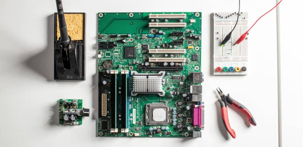
PCB assembly tips
PCB assembly and PCB manufacturing process are two very different PCB disciplines. Each of these two has its equipment and processes, and their complexity tends to differ. For example, PCB manufacturing involves fabricating a bare PCB, while PCB assembly involves placing various components on the bare PCB.
But how can you ensure that you always receive quality back once you submit your design for assembly? Just follow the following steps:
Use an IPC Certified Assembler
Institute for Printed Circuits, or IPC, is a worldwide organization that sets PCB assembly standards for PCB assemblers.
IPC certifications will ensure you get the best products from your PCB assembler each time. Therefore, this should be on your checklist when searching for an assembler.
Reconsider offshoring
Offshore assemblers offer tempting offers; however, working with local assemblers, in the long run, tends to be more beneficial. That is because offshoring leads to you incurring shipment costs, and if the PCB malfunctions fixing it will cost you more money. However, when you work with a local assembler, you can receive your PCB without incurring extra costs, and if the board malfunction, getting it fixed is not a hassle.
Work with the assembler
Do not wait up until the last minute to involver your PCB assembler. Instead, work with them from the very beginning. Doing so will help ease your designing process as you can quickly develop a PCB that the assembler can manufacture.
Utilize Consistent Labels
Labels are pretty crucial in PCB designs. Therefore, you should be pretty consistent in terms of the labels that you utilize. Moreover, double-check the PCB design document’s markings to make sure they all make sense.
Also, ensure you mark all the parts, do not leave room for guesswork.
Prioritize Features
Avoid creating a long disordered list of features for your PCB. Instead, create a prioritized list that contains high-priority features. You can then add in lower priority features later on.
File Formats
Always communicate with your PCB assembler at the early stages to learn whether or not they have experience in the file format you wish to utilize to make your PCB design. Skipping this step might lead to unnecessary delays later on.
Conclusion
Designing and assembling a printed circuit board tends to be a hassle for many people. Most people actually mess up and end up going over budget to compensate for design or assembly errors that they could have avoided. However, if you follow the tips in this article, you will generate a functional, optimized PCB without breaking a sweat.
