PCB pattern antennas are compact and cost-effective alternatives to traditional antennas. They are widely used in various wireless communication applications, such as RFID, Bluetooth, and Wi-Fi. These antennas are designed by etching a pattern on the copper layer of a printed circuit board (PCB), which allows them to transmit and receive radio frequency signals.
The design of a PCB pattern antenna depends on the frequency of the signal it needs to transmit or receive. The size and shape of the antenna pattern, as well as the distance between the pattern and the ground plane, affect the antenna’s performance. The antenna’s gain, bandwidth, and radiation pattern are important factors to consider when designing a PCB pattern antenna. By optimizing these parameters, engineers can create antennas that are efficient, reliable, and meet the requirements of their specific application.
Overall, PCB pattern antennas are a versatile and practical solution for wireless communication systems. They offer several advantages over traditional antennas, such as low cost, compact size, and ease of integration into PCB designs. As wireless communication continues to grow in importance, the demand for high-performance PCB pattern antennas is likely to increase.
What is a PCB Pattern Antenna?
A PCB pattern antenna is a type of antenna that is printed on a printed circuit board (PCB). It is a cost-effective and space-efficient solution for wireless communication devices. PCB pattern antennas are designed to transmit and receive radio frequency (RF) signals. They are widely used in a variety of applications, including mobile phones, laptops, tablets, and other wireless devices.
A PCB pattern antenna consists of a conductive trace or a series of traces on a PCB. The trace is designed to resonate at a specific frequency, which makes it capable of transmitting and receiving RF signals. The size and shape of the trace determine the frequency at which the antenna resonates. PCB pattern antennas can be designed to operate at various frequencies, depending on the application requirements.
One of the advantages of using a PCB pattern antenna is that it can be integrated into the PCB of the device, which saves space and reduces the overall cost of the device. PCB pattern antennas can also be designed to have directional or omnidirectional radiation patterns, depending on the application requirements. Additionally, they can be designed to have high gain, which increases the range and reliability of wireless communication.
In summary, a PCB pattern antenna is a type of antenna that is printed on a PCB. It is a cost-effective and space-efficient solution for wireless communication devices. PCB pattern antennas can be designed to operate at various frequencies, have directional or omnidirectional radiation patterns, and have high gain.
Design Considerations
When designing a PCB pattern antenna, there are several considerations to keep in mind to ensure optimal performance. The following sub-sections discuss some of the key design considerations.
Substrate Material
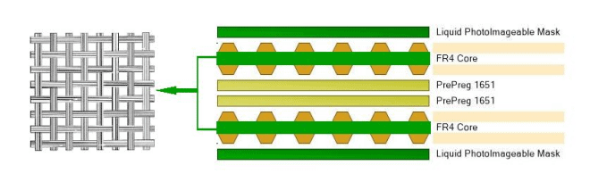
The choice of substrate material is crucial in determining the performance of the PCB pattern antenna. The substrate material should have a high dielectric constant to achieve a high radiation efficiency. Commonly used substrate materials include FR-4, Rogers, and Teflon. The choice of substrate material also depends on the operating frequency and the size of the antenna.
Trace Width and Spacing
The trace width and spacing determine the impedance of the antenna and its bandwidth. A narrow trace width and spacing result in a higher impedance, while a wider trace width and spacing result in a lower impedance. The trace width and spacing should be chosen carefully to match the desired impedance and to ensure good signal transmission.
Ground Plane Size
The ground plane size is another important consideration in the design of the PCB pattern antenna. The ground plane should be large enough to provide a low impedance path for the return current and to minimize the radiation from the feedline. The ground plane size should be at least half the wavelength of the operating frequency.
Feedline Design
The feedline design is critical in achieving good signal transmission and minimizing losses. The feedline should have a low impedance to match the impedance of the antenna and to minimize signal reflections. The feedline should also be designed to minimize losses due to radiation and dielectric losses.
In conclusion, the design considerations discussed above should be carefully considered when designing a PCB pattern antenna to ensure optimal performance. By choosing the right substrate material, trace width and spacing, ground plane size, and feedline design, one can achieve a high radiation efficiency and good signal transmission.
Simulation and Testing

Simulation Software
To design and optimize a PCB pattern antenna, simulation software is a critical tool. There are several simulation software options available, including HFSS, CST Microwave Studio, and FEKO. These software packages enable designers to simulate and analyze the electromagnetic performance of the antenna before fabrication.
Simulation software provides designers with a range of tools to analyze the antenna’s performance, including radiation patterns, gain, impedance matching, and bandwidth. Furthermore, simulation software allows designers to modify the antenna’s geometry and parameters to optimize its performance.
Testing Equipment
After designing and simulating the antenna, it is essential to test the antenna’s performance to validate the simulation results. Testing equipment includes network analyzers, spectrum analyzers, and anechoic chambers.
Network analyzers measure the antenna’s impedance and S-parameters, while spectrum analyzers measure the antenna’s radiation pattern and gain. Anechoic chambers provide an environment free from external interference, allowing accurate measurement of the antenna’s performance.
In addition to testing the antenna’s performance, it is also essential to test the antenna’s durability and reliability. Environmental testing, such as thermal cycling and vibration testing, can ensure the antenna’s performance under extreme conditions.
In conclusion, simulation software and testing equipment are critical tools in designing and optimizing a PCB pattern antenna. These tools enable designers to simulate and analyze the antenna’s performance before fabrication and validate the simulation results through testing.
Applications
PCB pattern antennas are widely used in various applications due to their compact size, low cost, and high efficiency. Some of the most common applications are:
Wireless Communication
PCB pattern antennas are commonly used in wireless communication devices such as smartphones, tablets, laptops, and routers. They provide reliable and efficient wireless connectivity for data transmission, voice communication, and internet browsing. PCB pattern antennas are also used in wireless sensors, RFID tags, and other IoT devices.
IoT Devices
The Internet of Things (IoT) is a rapidly growing field that requires small, low-power, and low-cost antennas for wireless communication. PCB pattern antennas are ideal for IoT devices because they can be integrated into the PCB layout, reducing the size and cost of the device. PCB pattern antennas can be used in smart home devices, wearables, healthcare devices, and industrial IoT applications.
Automotive Industry
PCB pattern antennas are increasingly used in the automotive industry for wireless communication, GPS navigation, and entertainment systems. They provide high performance and reliability in harsh environments such as extreme temperatures, vibration, and electromagnetic interference. PCB pattern antennas can be integrated into the car’s body, reducing the need for external antennas and improving the aesthetics of the car.
In conclusion, PCB pattern antennas have a wide range of applications in various industries due to their compact size, low cost, and high efficiency. They provide reliable and efficient wireless connectivity for wireless communication, IoT devices, and the automotive industry.
Advantages and Disadvantages

Advantages
PCB pattern antennas have several advantages over other types of antennas. Here are some of the key benefits:
- Low Cost: PCB pattern antennas are relatively inexpensive to manufacture, especially when compared to traditional antennas that require specialized equipment and materials.
- Compact Size: PCB pattern antennas can be designed to be very small, making them ideal for use in portable devices like smartphones and tablets.
- Customizable: PCB pattern antennas can be easily customized to meet the specific needs of a particular application. This is because the antenna design is integrated into the PCB layout, which can be easily modified using computer-aided design (CAD) software.
- Good Performance: PCB pattern antennas can provide good performance in terms of gain, efficiency, and radiation pattern. This is because the antenna is designed to be an integral part of the PCB, which can help to minimize losses and optimize performance.
Disadvantages
Despite their many advantages, PCB pattern antennas also have some disadvantages that should be taken into consideration:
- Limited Bandwidth: PCB pattern antennas typically have a limited bandwidth, which means that they may not be able to cover a wide range of frequencies. This can be a problem in applications where a broad frequency range is required.
- Susceptible to Interference: PCB pattern antennas are more susceptible to interference from other electronic components on the PCB. This can result in degradation of the antenna’s performance, especially if the antenna is located close to other components that generate electromagnetic interference (EMI).
- Design Complexity: PCB pattern antennas require a certain level of design expertise to ensure that they are optimized for performance. This can be a challenge for designers who are not familiar with antenna design principles.
Overall, PCB pattern antennas are a viable option for many applications, but they are not without their limitations. Careful consideration of the advantages and disadvantages is necessary to determine whether a PCB pattern antenna is the right choice for a particular application.
