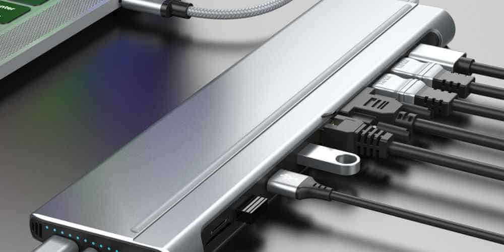
The USB-C connector is becoming increasingly popular in modern electronic devices. This connector is known for its versatility and compatibility with a wide range of devices. However, designing a printed circuit board (PCB) layout for the USB-C connector can be challenging.
One of the main challenges of designing a PCB layout for the USB-C connector is ensuring that the connector is properly grounded. This is important because USB-C supports high-speed data transfer and power delivery, which can create electromagnetic interference (EMI) if the connector is not properly grounded. Another challenge is ensuring that the connector is properly shielded to prevent EMI from interfering with other components on the PCB.
To overcome these challenges, designers must carefully consider the layout of the USB-C connector and the surrounding components. They must also take into account the specific requirements of the device and the intended use of the USB-C connector. With careful planning and attention to detail, designers can create a PCB layout that meets the requirements of the USB-C connector and ensures reliable performance.
USB C Connector PCB Layout Basics
Understanding USB C Connectors
USB Type-C is a reversible connector that can be plugged in either way, making it more convenient for users. It has 24 pins and supports various protocols like USB 3.1, DisplayPort, HDMI, and Thunderbolt 3. The connector’s small size and high-speed data transfer capabilities make it a popular choice for modern electronic devices.
USB C Connector Pinout
The USB Type-C connector has 12 pins on each side, with the pins arranged in a symmetrical pattern. The pins are divided into four groups: power and ground, USB 2.0 data, USB 3.1 data, and alternate modes. The power and ground pins are used to provide power to the device, while the data pins are used to transfer data.
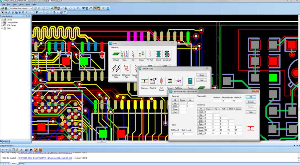
USB C Connector PCB Layout Guidelines
When designing a PCB layout for a USB Type-C connector, it is important to follow certain guidelines to ensure that the connector works properly. Here are some guidelines to keep in mind:
- Place the connector as close to the edge of the PCB as possible to allow for easy access.
- Keep the traces between the connector and the ICs as short as possible to minimize signal loss.
- Use a four-layer PCB to ensure proper grounding and signal integrity.
- Use a differential pair routing for high-speed signals to minimize crosstalk and noise.
- Place decoupling capacitors near the connector to reduce noise and improve signal quality.
By following these guidelines, you can ensure that your USB Type-C connector works properly and provides reliable data transfer and power delivery.
USB C Connector PCB Layout Considerations

When designing a printed circuit board (PCB) with a USB-C connector, there are several considerations that must be taken into account to ensure proper functionality and compliance with industry standards. This section will cover some of the key considerations for USB-C connector PCB layout, including signal integrity, power delivery, and EMI/EMC considerations.
Signal Integrity Considerations
Signal integrity is critical for USB-C connectors as it affects the overall performance of the device. To ensure good signal integrity, the following considerations should be taken into account:
- Proper termination of high-speed signal lines
- Minimization of trace lengths
- Use of controlled impedance routing
- Proper grounding and shielding of the connector
- Minimization of vias and other signal discontinuities
Power Delivery Considerations
USB-C connectors support a wide range of power delivery capabilities, including fast charging and high-power applications. To ensure proper power delivery, the following considerations should be taken into account:
- Proper selection of power components, including connectors, cables, and power management ICs
- Proper layout and routing of power traces to minimize voltage drop and power loss
- Use of proper decoupling capacitors to filter out noise and ensure stable power delivery
- Proper thermal management to prevent overheating of power components
EMI/EMC Considerations
EMI/EMC (electromagnetic interference/electromagnetic compatibility) considerations are critical for USB-C connectors as they affect the overall electromagnetic performance of the device. To ensure good EMI/EMC performance, the following considerations should be taken into account:
- Proper grounding and shielding of the connector and associated components
- Use of proper filtering components, such as ferrite beads and common-mode chokes
- Proper layout and routing of signal and power traces to minimize cross-talk and interference
- Use of proper grounding techniques, such as star grounding and separation of analog and digital grounds
In summary, proper USB-C connector PCB layout is critical for ensuring good signal integrity, power delivery, and EMI/EMC performance. By taking into account the considerations outlined above, designers can ensure that their USB-C PCB designs are compliant with industry standards and perform optimally.
USB C Connector PCB Layout Best Practices
Routing USB C Signals
When routing USB C signals, it is important to keep the differential pairs as close together as possible to minimize noise and crosstalk. The differential pairs should also be routed with equal lengths and impedance to ensure proper signal integrity. It is recommended to use 90-degree angles instead of 45-degree angles to reduce reflections.
Placement of USB C Connector on PCB
The placement of the USB C connector on the PCB is critical to ensure proper signal integrity and mechanical stability. It is recommended to place the USB C connector on the edge of the PCB to minimize the length of the traces and reduce noise. The placement of the connector should also be such that it is easily accessible for the user.
USB C Connector Traces and Via Considerations
The traces and vias used for the USB C connector should be designed to minimize signal loss and noise. It is recommended to use wider traces for the power and ground connections to reduce resistance and inductance. The vias used for the USB C connector should also be designed to minimize impedance discontinuities and signal reflections.
In conclusion, following these best practices can help ensure proper signal integrity, mechanical stability, and reliability of the USB C connector on the PCB.
Conclusion
In conclusion, designing a PCB layout for a USB-C connector requires careful consideration of several factors. These include the pinout, trace routing, power delivery, and signal integrity. It is essential to follow the USB-C specifications to ensure compatibility with other devices and prevent damage to the connector.
When designing the layout, it is crucial to keep the signal traces as short as possible and avoid crossing power and ground traces to reduce noise and interference. Placing decoupling capacitors near the connector can help filter out high-frequency noise and improve signal quality.
Additionally, it is essential to ensure that the power delivery system can handle the required voltage and current levels. The USB-C connector supports up to 100W of power delivery, which requires careful consideration of the power delivery network’s design.
Finally, testing the PCB layout thoroughly is critical to ensure that it meets the USB-C specifications and works correctly with other devices. This includes testing for signal integrity, power delivery, and compatibility with different USB-C devices.
Overall, designing a PCB layout for a USB-C connector requires a thorough understanding of the USB-C specifications and careful consideration of several factors. By following best practices and testing thoroughly, it is possible to create a reliable and compatible USB-C connector PCB layout.
